Quantcast
Channel: Analog : operational amplifier
Viewing all 408 articles
Browse latest View live

“Trust, but verify” SPICE model accuracy, part 2: input offset voltage vs. input common-mode voltage

$
0
0

It’s no secret that low-voltage rail-to-rail input operational amplifiers (op amps) are gradually taking the place of traditional high-voltage amplifiers in many precision applications. Rail-to-rail input amplifiers are extremely useful, since their linear input-voltage range spans the entire power-supply voltage range (or even beyond). They traditionally achieve this span through the use of two pairs of input transistors instead of one pair, but you should be mindful of new design challenges that this topology creates.

One challenge is the change in the op amp’s input offset voltage (VOS) when the amplifier input stage crosses over from one pair of transistors to another. This phenomenon is often called input crossover distortion. VOS is an important performance characteristic of a precision op amp, and many systems must calibrate out the initial offset voltage to meet their performance goals. Any changes to VOS, whether caused by changes in input common-mode voltage (VCM), temperature or other variables, are highly undesirable and can throw off a system’s total error performance. Figure 1 gives an example of VOS changing dramatically with increased VCM.

 Figure 1: VOS vs. VCM

When using SPICE simulation for rail-to-rail input amplifier designs, it’s wise to check that the VOS vs. VCM behavior of your models matches the real devices. Figure 2 shows the recommended test circuit.

 Figure 2: VOS vs. VCM test circuit

This simple circuit places the op amp in a unity-gain buffer configuration to prevent output swing limitation issues, then sweeps VCM to determine the change in VOS. To plot VOS vs. VCM, run a DC transfer characteristic while stepping VCM across the entire supply voltage range and measure VOS across the op amp input pins as shown in Figure 2.

Let’s use this method to test the response of the OPA388, a new zero-crossover precision amplifier from TI that uses a charge pump in its input stage to achieve true rail-to-rail performance using only a single transistor pair. This eliminates the input crossover distortion found in traditional rail-to-rail input op amps. See Figure 3.


Figure 3: VOS vs. VCM results of the OPA388

The simulated results match the responses of the three test devices given in the OPA388 data sheet very closely, with a change of less than 1μV over the entire VCM range.

Let’s use the same test circuit to check the response of the OPA2325, another zero-crossover precision amplifier from TI. See Figure 4.


Figure 4: VOS vs. VCM results for the OPA2325

Again, the simulated results match the real silicon very well. Keep in mind that while the simulation model looks like it has higher offset than the real silicon, all of the test devices measured in this plot had a VOS lower than the typical spec of 40μV, while the SPICE model was designed to match the typical.

Thanks for reading the second installment of the “Trust, but verify” blog series! In the next installment, I’ll discuss how to measure open-loop output impedance and small-signal step response to perform stability analysis. If you have any questions about simulation verification, log in and leave a comment, or visit the TI E2E™ Community Simulation Models forum.

Additional resources


Three reasons why a bidirectional I/O will simplify your next 4K video design

$
0
0

As 4K video becomes the norm for the professional video industry, high-quality serial digital interface (SDI) components and meticulous board layout are imperative for a high-performance end product. In addition, flexibility, scalability and cost savings are necessary to maximize design reuse, whether you are looking to expand your 12G product portfolio or aiming to transition from 3G-SDI to 12G-SDI.

A bidirectional input/output (I/O) addresses these critical needs. A bidirectional I/O is a device that you can configure as either a receive cable equalizer or a transmit cable driver through the same port. Let’s look at how this flexible device simplifies 4K video interfaces.

Reason No. 1: To enable design flexibility

Traditionally, SDI designs have a fixed number of input and output ports. Since cable equalizers and cable drivers are not interchangeable at the same port, designing a new system is necessary whenever you require a different combination of inputs and outputs. With a bidirectional I/O, you can easily support multiple configurations of inputs and outputs with the same design, as illustrated in Figure 1.

Figure 1: With a bidirectional I/O, a single design supports multiple input and output port configurations

TI’s latest 12G bidirectional I/O, the LMH1297, also enables dynamic port provisioning, meaning that end users can configure the port as an input or output on the fly. This design flexibility and scalability reduces both overall development time and the cost of stocking unique boards to support each port-configuration combination.

Reason No. 2: To minimize board space and bill-of-materials cost

In a traditional design, two ports support input and output functionality, resulting in a four-chip solution. A bidirectional I/O minimizes board space by reducing the overall number of ports. With a bidirectional I/O, you only need one port, and thus a single-chip solution. Comparing these two design approaches in Figure 2, a bidirectional I/O significantly reduces the number of board components.

Figure 2: TI’s bidirectional I/O reduces the overall number of ports, while its on-chip integration reduces the number of external passive components required.

TI’s new 12G bidirectional I/O takes minimization and cost savings a step further. The LMH1297 has an integrated reclocker, return loss network and terminations. The integrated reclocker ensures a clean output signal with minimal jitter. Meanwhile, the integrated return loss network and terminations eliminate the need for an external return loss network, not to mention time spent fine-tuning these network parameters.

The LMH1297 integrates an additional 75Ω loop-through cable driver output and a 100Ω loopback printed circuit board (PCB) driver output. You can use these additional outputs to expand signal distribution efficiently and improve system diagnosis capability, without extra cable drivers or reclockers to support the same system functionality. Applications for the additional loop-through and loopback driver are shown in Figure 3.

Figure 3: The additional driver outputs in the LMH1297 simplify signal distribution when the I/O is configured as either an input (EQ Mode) or output (CD Mode).

Furthermore, TI’s bidirectional I/O is implemented on a single-die solution. Traditionally, bidirectional I/Os are designed as a multichip module (MCM), which adversely affects overall performance compared to a stand-alone cable equalizer or cable driver. With the single-die approach, the LMH1297 achieves performance equivalent to or exceeding that of many other stand-alone cable equalizers and drivers. These features are offered in a 5mm-by-5mm very thin quad flat no-lead (WQFN) package.

Reason No. 3: To provide an easy upgrade path

Before taking your first steps to designing with a bidirectional I/O, it is worth considering whether alternative upgrade options are available to prepare current designs for the next generation. As the SDI community trends upward from 3G-SDI to 12G-SDI, having a pin-compatible upgrade path makes sense to minimize board redesigns and future-proof your products.

The LMH1297 comes with several pin-compatible alternatives in an identical package for easy upgrade. These alternatives are also software compatible. As shown in Figure 4, the LMH0397 is a 3G bidirectional I/O with an integrated reclocker, while the LMH1228 and LMH1208 are 12G dual cable drivers.

Figure 4: LMH1297 pin and software compatible portfolio

Why re-invent the wheel for each project? Maximize your efficiency and simplify your next SDI design with a bidirectional I/O.

To learn more about new interface products and get an edge in your 4K transition, visit TI’s SDI portfolio or log in to post a comment below or talk with other engineers in the TI E2E™ Community High Speed Interface forum.

Additional resources

Speed up basic circuit design with the analog engineer’s calculator

$
0
0

Quick quiz: Can you find the standard 1% resistor values for a voltage divider that comes closest to a divider ratio of VOUT/VIN = .3278, with less than 0.01% error? The answer is 324Ω and 158Ω, with 0.00025% error.

Setting up the equation to solve for one of the values in terms of the other is easy. But iterating through multiple standard resistor values is tedious and time consuming, even when using a spreadsheet.

The analog engineer’s calculator simplifies this task. This newly developed tool is a companion to the “Analog Engineer’s Pocket Reference.” Many of you are familiar with this e-book, which covers many fundamental topics in circuit design: unit conversion, components, circuit equations, op amps, printed circuit board (PCB) design, sensors and analog-to-digital converters (ADCs). For those of you who hate memorizing even basic formulas and equations (or more likely, have gotten a little rusty), the pocket reference is an easily accessible source that can save tons of time (unless, of course, you have meticulously indexed your college textbooks).

This beta tool contains a collection of simple-to-use calculators that support much of the content in the pocket reference. While it doesn’t address every topic, it does cover the more interesting and complex topics, and constitutes one-stop shopping for many of the simple calculations that you might perform regularly. Figure 1 lists the possible calculations.

Figure 1: Analog engineer’s calculator menu

The calculator is especially useful when designing sensor signal-conditioning and data-acquisition systems to monitor voltage, current and temperature. The built-in calculators for amplifiers, data converters and temperature sensors make the task easier and faster. Need to design an input drive circuit for a successive approximation register analog-to-digital converter (SAR ADC)? Use the ADC SAR drive calculator to design the circuit. As Figure 2 shows, simply select the input type (single ended, differential, etc.); enter the ADC resolution, sampling cap value, full-scale input range and acquisition time; and click OK to see the associated resistor-capacitor circuit values, as well as other parameters.

Figure 2: ADC SAR drive calculator

Analog designers often need to make cascaded noise calculations when selecting circuit components to meet target specifications. Setting up signal-chain noise calculations can be tedious, but the calculator enables quick computations using only a few input parameters, as shown in Figure 3.

Figure 3: ADC plus signal-chain noise calculation

How many times have you designed a simple inverting or noninverting gain stage and wanted to get as close as possible to your target gain using only standard 1% resistors? You probably know that breaking up the feedback resistance into two or more discrete values reduces the error caused by the resistor tolerances. Selecting the 1% resistor values and calculating the actual gain and gain error isn’t difficult, just tedious. You have more important things to do. Use the amplifier gain resistor calculator to speed up the task (Figure 4).

Figure 4: Gain resistor calculator

Perhaps you need to calculate the inductance and capacitance of a section of PCB trace. Use the microstrip calculator to quickly find these values by entering a few trace parameters (Figure 5).

Figure 5: Microstrip calculator

These examples represent just a few of the often-used analog design calculations, aggregated into a single tool that you can place on your desktop and access offline. No more bouncing between bookmarks on the web. Download the “Analog Engineer’s Pocket Reference” and test out the analog engineer’s calculator to begin exploring the useful features that will speed up basic design tasks and save you valuable time. Sign in and comment below if you have any feedback or suggestions about the calculator. 

Additional resources

IO-Link: The backbone of the smart factory

$
0
0

You’ve likely heard of the Internet of Things (IoT) and how it not only connects your internet-enabled devices to each other, but enables them to communicate and share data to improve your quality of life. Today, the manufacturing industry is using the IoT as a key piece of the next wave of manufacturing. Industry 4.0, which is a word some have coined to mean the next industrial revolution, describes factory automation and the ability to construct a “smart factory” where data is easily exchanged and harnessed to keep factories running at maximum efficiency. IO-Link is an important interface to implement this factory transition.

You may think that factories are already efficient based on the quality of products you buy today and the price at which you can purchase them. In reality, factories have numerous inefficiencies that an interface like IO-Link can help reduce. The IO-Link Consortium and International Electrotechnical Commission (IEC) 61131-9 standard established a bidirectional, manufacturer-independent communication protocol for sensors and actuators. The specification also defines a mechanical interface that is fully backward-compatible with existing field buses, such as Profibus, Profinet and EtherCAT, used today.

Let’s look at few key advantages of IO-Link and how they are helping drive factory automation:

  • Bidirectional communication. Today’s factories primarily use one-way sensors, meaning that they only provide data based on standard input/output (SIO)/digital output switches. So if a red wagon in a toy factory comes down the line painted green, the one-way sensor alerts engineers of the fault. But that isn’t helpful if someone actually ordered a green wagon. IO-Link’s bidirectional protocol enables factories to easily update sensor parameters, enabling custom orders without going to the factory floor to reprogram each sensor. Bidirectional communication also provides factories real-time information about cable breaks, overtemperature conditions, output shorts and transfer diagnostics. In some cases, the sensor can even alert the factory that it is nearing its end of life.
  • Manufacturer-independent. Manufacturers who follow the IO-Link standard will produce sensors and actuators that operate, not only with their other products (sensors, programmable logic controllers [PLCs]), but with competitor solutions. A standard interface, cable and connector gives factories the ability to develop a process that delivers products based on their key requirements, while maintaining a high level of efficiency and flexibility.
  • Communication protocol. IO-Link’s point-to-point communication protocol enables up to 32 bytes depending on the required cycle time. Additionally, the IO-Link master can store sensor and timing parameters. This key feature enables engineers to easily switch out faulty sensors and download parameters to the new sensor automatically, further reducing downtime and increasing factory efficiency.
    • Backward compatibility. As I mentioned, SIO/digital output switches are the primary interface to the PLC today. There are many SIO sensors installed in factories today, and the thought of replacing them with a new technology is an overwhelming one. The IO-Link authors recognized this and mandated that the connector for IO-Link must use not only the same connector/pinout as the installed base, but also the same cabling, so that manufacturers could easily update their factory lines.

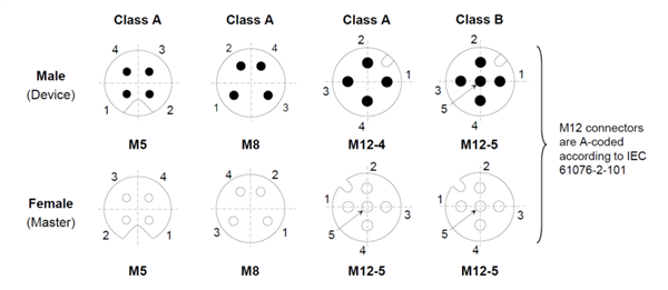
These connectors, as shown in Figure 1, are based on the specifications outlined in IEC 61131-9. They are the same (M5, M8 and M12 type) connectors used throughout installations today.

Figure 1: IO-Link SIO connectors

Connections can occur across a three-wire (or more) cable stretching to a maximum of 20 meters (66 feet). Table 1 defines the IO-Link signals.

* Required for three-wire interface Table 1: IO-Link cable definitions

If you’re familiar with SIO, you’ll notice that its functions are the same as those listed in the table, with VCC, OUT and GND usually referenced. Both IO-Link and SIO use the C/Q (or OUT) signal for data.

TI has shipped IO-Link-enabled transceivers since 2011 and recently released its second generation of transceivers. In my next blog post, I’ll talk about how our TIOL111 IO-Link device transceiver and TIOS101 digital output switch further enable smart factories.

Additional resources

“Trust, but verify” SPICE model accuracy, part 3: slew rate and input clamping diodes

$
0
0

Previous installments of this blog post series discussed the need to verify SPICE model accuracy and how to measure common-mode rejection ratio (CMRR) and offset voltage versus common-mode voltage (VOS vs. VCM). In part 3, I’ll continue by explaining how to verify an operational amplifier (op amp) model’s slew rate, which is a large-signal output response.

Slew rate

Slew rate is defined as the maximum rate of change of an op amp’s output voltage and is typically given in volts per microsecond (V/µs). Slew rate is a type of output distortion, or nonlinearity. An amplifier in this condition is not behaving linearly where the output voltage equals the input voltage multiplied by the closed-loop gain. Instead, the op amp output voltage changes with a constant slope. This continues until the op amp corrects the difference at its input pins and the amplifier returns to a linear or small-signal operating state. For a more detailed look at slew rate, watch our TI Precision Labs – Op Amps video series on slew rate.

One of the most common ways to force an op amp into slew rate limit is to apply a large-signal input step of 100mV or greater, but slew limiting can also occur when trying to output high-amplitude signals at high frequencies. In audio applications, for example, slew limiting distorts sine waves into triangle waves, causing visible (and audible) distortion, as shown in Figure 1.

 Figure 1: Triangular distortion caused by slew rate limit

When using SPICE simulation for audio applications or circuits where large-signal input steps are common (such as those with multiplexers or switches), I recommend verifying the slew rate behavior of your op amp model. Figure 2 shows the recommended test circuit.

 Figure 2: Slew rate test circuit

This circuit places the op amp in a unity-gain buffer configuration and applies a large-signal step to the noninverting input pin. The amplitude of the step should match the test conditions given in your specific op amp’s data sheet.

Let’s test the slew rate of the OPA196, a new e-TrimTM precision amplifier from TI, whose data sheet specifies a 10V input step test condition (Figure 3). To determine the slew rate, measure VOUT and calculate its rate of change as it transitions from 10% to 90% of the total output step.

 Figure 3: Slew rate test results for the OPA196

Equations 1 through 3 calculate the rising slew rate for the OPA196:

 where ΔV is the change in voltage and Δt is the change in time from 10% to 90% of the output transition. In this case, the simulated rising slew rate perfectly matches the data sheet spec of 7.5V/µs! You can repeat this test with a negative input step to measure the falling slew rate.

Testing amplifiers with input clamping diodes

Testing the slew rate of certain types of amplifiers requires a small tweak to the slew rate test circuit. On most bipolar, high-voltage complementary metal-oxide semiconductor (CMOS) and chopper amplifiers, clamping diodes are present across the op amp input pins. If you try to apply a large-signal step to these devices, the large differential input voltage will cause these diodes to conduct current directly from the noninverting input to the inverting input and output. The result is an incorrect slew rate measurement that’s faster than what the actual device can generate. Figure 4 shows this effect with the OPA1678, a high-voltage CMOS audio amplifier from TI.

 Figure 4: Slew rate test results (no input current limit) for the OPA1678

This effect was not evident on the OPA196, even though it’s a high-voltage CMOS amplifier. That’s because it’s part of TI’s OPA19x family of amplifiers with multiplexer-friendly inputs. The design of the OPA19x family eliminates the need for input clamping diodes, and the amplifiers can handle large differential input voltages without them. Junction field-effect transistor (JFET)-input amplifiers such as the OPA145 also do not exhibit this issue.

To test the true slew rate of amplifiers with input clamping diodes, place a current-limiting resistor either in series with the input source or between the inverting input and the output pin. A resistance of 10kΩ does the trick for the vast majority of op amps. Figures 5 and 6 show the modified circuit and test results.

 Figure 5: Slew rate test circuit with input current limit


 Figure 6: Slew rate test results with input current limit for the OPA1678

Using Equations 1-3 once more, the rising slew rate of the OPA1678 model is 8.9V/µs – very close to the data sheet spec of 9V/µs.

As an alternative to using a large input current-limiting resistor, you can test the slew rate with the amplifier in an inverting configuration. In this case, the input and feedback resistors limit the input current through the input diodes and enable an accurate measurement.

Thanks for reading the third installment of the “Trust, but verify” blog series! In the next installment, I’ll discuss how to measure open-loop output impedance and small-signal step response to perform stability analysis. If you have any questions about simulation verification, log in and leave a comment, or visit the TI E2E™ Community Simulation Models forum.

Additional resources

Save

Is your factory smarter than a fifth grader?

$
0
0

In my last post, I discussed the future of factory automation and how IO-Link is an enabling interface for Industry 4.0. You can use the IO-Link bidirectional, manufacturer-independent communication protocol to develop highly efficient and scalable “smart factories.”

TI’s TIOL111 IO-Link transceiver and TIOS101 digital output switch will enable the next generation of sensors and actuators in factories, while providing features that further optimize product offerings and simplify bill of materials.

You can take advantage of the pin compatibility between the TIOL111 and TIOS101 devices to develop a complete portfolio of both IO-Link and standard input/output (SIO) enabled sensors without using two separate printed circuit boards (PCBs) for each offering. Each device supports the interfaces intended while also supporting a high level of integrated protection, including:

  • 16kV International Electrotechnical Commission (IEC) 61000-4-2 electrostatic discharge (ESD).
  • 4kV IEC 61000-4-4 electrical fast transient (EFT) Criterion A.
  • 1.2kV/500Ω IEC 61000-4-5 (surge).
  • ±65V transient tolerance.
  • Reverse polarity up to ±55V.
  • Overcurrent/overvoltage/overtemperature.

This level of protection can simplify designs by eliminating or greatly reducing the size of external transient voltage suppression (TVS) diode components that originally provided protection, thus reducing the overall bill of materials and associated costs when compared to previous-generation or competitive solutions.

The physical size of sensors continues to shrink. The smallest of these sensors is likely the cylindrical sensor, as shown in Figure 1.

Figure 1: IO-Link cylindrical sensor

The sensor at the top of Figure 1 is the finished product with a cylindrical enclosure. The middle wire is the sensor’s internal printed circuit board (PCB). This PCB measures 17.5mm by 2.5mm. In order to fit in these small form factors, an equally small device is required to implement either IO-Link or SIO output. Knowing these system requirements drove a new package development for TIOL111 and TIOS101 solutions. The DMW package is one of the smallest, thermally enhanced IO-Link packages available today. Measuring 3.0mm by 2.5mm, the DMW package also supports a thermal pad for heat conduction and a flow-through pinout. The flow-through pinout (Figure 2) further aides in PCB layout and device placement by supporting the logic interface to the microcontroller on one X-axis and the 24V IO-Link interface on the other.

Figure 2: TIOL111/TIOS101 flow-through package

The TIOL111 and TIOS101 have a low residual voltage of just 1.75V – the size of sensors that use IO-Link and SIO are rugged, sealed and often very small. This small, enclosed form factor introduces numerous design challenges, with thermal performance one of the most challenging. By supporting an ultra-low residual voltage of 1.75V at 250mA, the TIOL111 and TIOS101 provide a superior base for power dissipation and related system thermal management.

Table 1: Power dissipation = residual voltage × 10

Configurable current limit is an additional protection feature that can protect the sensor and possibly prevent the network from shutting down. Through a 0-100kΩ resistor, the TIOL111 and TIOS101 can support a 50-350mA current limit. This limiter can notify the programmable logic controller (PLC) of an overcurrent condition and shut down the device's output, with periodic monitoring of the overcurrent condition.

The configurable current-limit resistor is placed on the ILIM_ADJ pin (see Figure 3). 

Figure 3: TIOL111 application schematic

As Figure 4 indicates, using a 0Ω resistor on the ILIM_ADJ pin will default to the maximum current limit of 350mA (see Figure 4)

Figure 4: Current limit vs. RSET

These and other features and benefits of the TIOL111 and TIOS101 can enable the smallest sensor form factors, while providing the flexibility to support multiple platforms and current configuration requirements.

Additional resources

How ultrasonic technology improves convenience and performance in home automation

$
0
0

Homeowners are becoming more interested in automating the control of lights, fans, thermostats, TVs, music equipment, garage doors, doorbells and much more, leading to a growing trend of bringing commercial building automation technologies home. Amazon Alexa, Google Home, Apple HomePod and HomeKit, Wink, and a multitude of other central hubs control and monitor various electrical/electronic devices in a home, as shown in Figure 1.

Figure 1: Popular home automation products with motion or presence detection

The challenge with home automation is that this technology is in the early stages of evolution; thus, some central hubs work effectively and some do not. Home automation central hub and device manufacturers are continuously innovating to improve performance and enhance convenience, while also seeking to reduce energy consumption.

What most products need is a way to detect the early presence or approach of people nearby, while otherwise remaining in sleep mode and conserving power. Upon detection, these devices automatically wake up and perform key functions, like turning lights on or off; adjusting heating, ventilation and air-conditioning (HVAC) system settings; turning on electronic doorbells before they’re pressed and notifying homeowners (or recording video); or activating burglar alarms.

Motion detectors are generally based on optical, microwave or acoustic technology. The most popular is passive infrared (PIR) optical technology. But in this blog post, I’m going to talk about ultrasonic acoustic technology.

You might be asking yourself, “Why should I choose ultrasonic sensing for presence or motion detection over the more popular PIR sensors?” PIR sensors work on the principle of changes in temperature taking place in front of the sensor, but that means that insects or small animals can trigger them. Direct white light on a sensor can also momentarily “blind” it and trigger false alerts. Camera systems detect a change in images between frames to register motion, but again, insects or birds can trigger these systems; so can the movement of leaves and plants in view of the camera. Ultrasonic sensing is not susceptible to such false alarms as it is based on the principle of motion or presence of a target obstructing the transmitted sound waves and generating echoes that bounce back to the sensor. The strength of the echoes as a result of the presence of humans is different compared to insects or pets and the system can be programmed to detect the right kind of targets.

 Although multiple sensing technologies can detect the presence or approach of people, including optical time of flight and capacitive sensing; ultrasonic sensing is one of the lowest-cost and most versatile technologies. While currently used extensively in automotive park-assist systems for obstruction/presence detection, you can also leverage ultrasonic sensing in central hubs, occupancy detection and advanced motion detectors.

In many scenarios, the advantages of ultrasonic technology are not just cost, but performance as well. It works in different mediums, like air, water and gas. It can detect objects regardless of shape, size, color or surface contour. Like radar, it can create 3-D images of objects that enable systems to make better decisions, such as distinguishing between a house pet or a human. Finally, ultrasonic technology has a competitive price-to-feature benefit in end products.

The integration of an ultrasonic sensing-based presence detection subsystem into a home automation device will have an ultrasonic transducer directed in a specific direction or broadcast in a wide (90-135 degree) arc to detect an approaching person. Additional transducers can increase coverage to 360 degrees. Upon the detection of a presence from reflected ultrasonic waves, the output of this subsystem activates the device accordingly; for example, turning on the camera feature in a video doorbell or surveillance camera.

In systems like smart speakers, ultrasonic-based presence detection can turn on the specific microphones that are facing the approaching person, improving system accuracy. In other examples, an ultrasonic subsystem can turn on lighting or air conditioning in rooms upon the detection of humans and even replace the motion detectors used in home security systems.

Presence detection is, of course, not limited to home automation; it’s extendable to building automation as well. One fast-growing application is open parking-spot detection in garages at airports, malls and other commercial facilities. In this use case, an ultrasonic module placed above the parking spot or embedded in the ground detects the presence of a vehicle. Green or red lights mounted to the ceiling notify drivers whether the spot is open or occupied. An example module is shown in Figure 2 below which includes the PGA450-Q1 ultrasonic system on chip (SoC) interface IC and an ultrasonic transducer in a small form factor.

Figure 2: Small Form Factor Ultrasonic Sensing Module

Depending on the design requirements and associated costs, the parking-spot detector module can be wired or wireless. For a wired system, you only need a module similar to the reference design in Figure 2,  modified to include two light-emitting diode (LED) lights. Or, to avoid having cabling along the ceiling of the parking garage, you could opt for a wireless mesh network using one of many wireless standards such as Bluetooth®, Wi-Fi®, or Zigbee.

It’s possible to implement presence detection in many ways, but in my opinion the most cost-effective approach with the least amount of false alerts is an ultrasonic-based approach.

To get posts like this delivered to your inbox, sign in and subscribe to Analog Wire.

Additional resources

Unique active mux capability combines buffer and switch into one solution

$
0
0

This post is co-authored by Anthony Vaughan.

Designers often run into the problem of selecting one of two (or several) inputs to pass on to the next stage. While a plethora of multiplexer (mux)-type devices use a modified impedance approach to select which input passes to a single output, a new high-speed precision operational amplifier (op amp) adds this capability internally.

The OPA837 single-channel op amp includes a switch internal to the inverting node that operates along with the power shutdown feature. This enables simple active-mux operation, shown as the 2x1 example in Figure 1. The extremely low power operation of the 105MHz OPA837 device adds little to the system power budget (0.6mA/channel), while giving almost perfect isolation between channels and in the off-channel path.

Figure 1: Simple gain of 1, 2x1 active mux using two OPA837 op amps

In Figure 1, the two amplifiers are shown as a unity gain buffer. They can be configured in any gain or attenuation setting, but in addition to the output load, each amplifier will need to drive a parallel combination of the feedback and gain resistors for both channels.

The power shutdown feature operates off the negative supply. The LM7705 switched capacitor inverting regulator provides a fixed -0.23V negative bias supply voltage from a 3V to 5.25V input to give the necessary headroom on the output to operate true swing to ground. The OPA837 inputs are negative rail. A low-voltage ground-referenced logic signal and its inverted version will toggle between the two amplifiers, making one active at a time. Use break-before-make logic sequencing to avoid both outputs being active at the same time. If break before make is not possible, isolate the two outputs from high transition currents with 100Ω resistors in the outputs inside the feedback connection.

Pulling the power disable voltage below 0.32V on one channel will disable it, while raising it above +1.27V on the other will enable that channel. The -0.23V negative supply provided by the LM7705 has shifted these power disable voltage levels below the minimum/maximum range specific in the data sheet.

The rail-to-rail output stages used in the OPA837 go high impedance when disabled. What has been missing to make this active mux application work is a similar high impedance looking into the disabled channel’s inverting input pin. The OPA837 unity-gain stable voltage feedback op amp (VFA) is the first to provide an active switch to either connect or isolate the internal input stage transistor on the inverting input from the external world. When active, this switch is low impedance and inside the feedback loop, and thus transparent to normal op amp operation. The noninverting inputs remain very high impedance whether enabled or disabled.

A critical test of this active mux capability is a sweep of harmonic distortion for a simple single amplifier case, and then repeating that test with a disabled OPA837 connected to the active stage output. All previous amplifiers showed a nonlinear load vs. output voltage swing (Vpp) into the inactive inverting input, degrading harmonic distortion performance. Figures 2 and 3 show the transparent operation provided by this new active mux at 2Vpp I/O and 4Vpp I/O, respectively. The 4Vpp test (0V à 4V input) required a +5.2V supply to provide 1.2V of headroom at the input stage.

Figure 2: 2Vpp with and without an inactive stage connected to the output pin


Figure 3: 4Vpp with and without an inactive stage connected to the output pin

As these tests show, there was no degradation in harmonic distortion from the simple single amplifier test case.

How else could you use this new internal capability? Here are a few ideas:

  • Fan the active mux application to more than a 2x1. For a gain of 1, I recommend a capacitive load-isolating resistor in the feedback to limit the buildup of capacitive load on the active channel output. The parallel inactive inverting input capacitive loads can begin degrading the phase margin for the active channel.
  • Take a single source signal and create a simple n-bit digital variable gain amplifier (DVGA) by connecting the outputs of two or more OPA837 stages at different gain settings and selecting only one to be active at a time.

Figure 4 shows a simple 1-bit DVGA providing a gain of 1 or 2 to the output from a shared input signal.

 Figure 4: Selectable gain application of the input switch within the OPA837

When either path is active, the amplifiers will now need to drive the 4kΩ feedback load in parallel with the 2kΩ load shown in Figure 4. Figure 5 shows the two possible frequency response curves for Figure 4. Of course, a wider gain step is possible by setting one channel to a gain higher than 2V/V. There will be an increasing difference in bandwidths by doing that, however. A post-filter lower than the lowest stage bandwidth will hold the response shapes constant as different gain channels are selected.

Figure 5: 1-bit DVGA small-signal response shapes for a gain of 1 and 2 in the OPA837

You can use the OPA837 to solve your simple mux problems, adding some gain in the signal path if desired. Or you could extend your dynamic range by using the OPA837 to provide a simple switched gain stage. Both applications are well supported by the exceptional DC precision and low power of the OPA837. Learn more about single mux design in the E2E™ High Speed Amplifiers forum.

Additional resources

Save


Forget the tiny homes craze – Have you heard about tiny inductors for automotive Class-D amplifiers?

$
0
0

You can’t turn on the TV or open a website lately without seeing or reading about the tiny home craze. Smaller is supposedly better, right? Similarly, mobile phone manufacturers tout how small, slim or lightweight their next-generation phone is.

It just seems natural that this trend would spill over into the automotive audio Class-D amplifier space. So in this post, I’ll talk about how tiny inductors are used with Class-D amplifiers in infotainment systems.

Background

Automotive Class-D audio amplifier designs require a filter on the output of the amplifier. This filter uses both an inductor and a capacitor on each output terminal, usually referred to as an inductor-capacitor (LC) filter. Proper selection of the LC filter values is critical to meet the desired audio performance, efficiency, electromagnetic compatibility (EMC)/electromagnetic interference (EMI) requirements and cost, especially in automobile head unit and external amplifier applications.

The Class-D amplifier bridge-tied load circuit shown in Figure 1 is an output configuration where the speaker (or load) is connected between two amplifier outputs, bridging the two output terminals. Automotive Class-D audio amplifiers therefore typically require two inductors per channel (speaker).

Figure 1: Class-D amplifier bridge-tied load circuit

Why are tiny inductors important?

Automobile manufacturers are adding more electronic subsystems in today’s vehicles. Yet space is at a premium, so electronic module suppliers are under pressure to make their subsystems smaller. A secondary effect is that automobile manufacturers are continuously striving to make vehicles lighter weight to increase fuel efficiency. While there are many subsystems to evaluate, today I’d like to focus on comparing inductor sizes and weight as part of car radio designs within an infotainment system.

A typical car radio design has at least four channels to drive two front speakers and two rear speakers. This simple configuration would require eight total inductors for a Class-D automotive audio amplifier, since each channel requires two inductors, as shown in Figure 1. Thus, the size of each inductor is multiplied by eight, which is a significant contribution to overall printed circuit board (PCB) size and design weight.

Inductor size vs. amplifier switching frequency

For Class-D automotive audio amplifiers, the value of the inductor required in the LC filter to ensure the proper pulse-width modulation (PWM) demodulation filter characteristic depends on the switching frequency. In Figure 2, the inductor size used in LC filters for a typical Class-D audio amplifier design that switches around 400kHz are quite a bit larger and bulkier than those required for a newer Class-D amplifier design switching at a much higher frequency, such as 2.1MHz on TI’s TAS6424-Q1 device.

A 400kHz automotive audio amplifier typically uses either a 10µH or 8.2µH inductor value, while the 2.1MHz higher-switching-frequency amplifier design can take advantage of a much smaller and lighter-weight inductor in the range of 3.3µH to 3.6µH (assuming that each amplifier provides equivalent output power).

Figure 2: Comparison of inductor size vs. switching frequency

What drives inductor weight?

The weight difference between 8.2µH and 3.3µH inductors is mainly caused by the sheer difference in the weight of the copper windings and core material required to achieve the LC filter’s required inductance value and current-handling capability. As previously mentioned, a simple four-channel car radio design requires eight total inductors. In Figure 3, you can see the difference in weight (the total weight of copper and core material) of a four-channel radio design based on a 400kHz switching frequency versus one based on a 2.1MHz switching frequency.

Figure 3: Inductor weight differences for a typical four-channel amplifier

Newer metal-alloy inductors enable very small amplifier size

Inductors used in 400kHz switching frequency amplifier designs are traditionally made using copper wire and ferrite materials for the core. With the implementation of the higher 2.1MHz switching frequency, it’s possible to develop inductors with copper wire and a new metal-alloy core technology, which enables incredibly tiny inductor sizes. Figure 4 shows that the newer metal-alloy technology not only provides the lightest weight solution, but helps greatly reduce the overall solution size for a four-channel amplifier.

Figure 4: Tiny metal-alloy inductors for a typical four-channel amplifier

Conclusion

Higher-switching-frequency automotive Class-D audio amplifier designs, like the 2.1MHz TAS6424-Q1, are the way of the future to fulfill industry demands for next generation car radios and external amplifiers. The higher-switching-frequency amplifiers also help to drive technology advancement in the inductor industry, thereby helping to provide overall smaller and lighter weight system solutions. Want to know more about LC filter design? Download this application report for in-depth design information.

Additional resources

Body control modules – invisible but fundamental for every car

$
0
0

Electronics in vehicles are taking on more and more functions (safety, driver assistance, more driver information) and the demand for greater electronics content overall continues to accelerate. As features related to comfort, safety, equipment and a customized riding experience increase almost daily, so too do the requirements of the vehicle’s electrical system.

Body control modules (BCMs) coordinate different vehicle functions within a car through the use of signals. They manage numerous vehicle functions, including but not limited to door locks, chime control, interior and exterior lights, security functions, wipers, turn indicators and power management. Tied into the electronics architecture of the vehicle, BCMs reduce the number of plug-in connections and cable harnesses required while offering maximum reliability and economy.

As the demand for increased functionality in BCMs has grown, the amount of cable harnesses has increased as well. For example, according to Kiyotsugu Oba in “Wiring Harnesses for Next Generation Automobiles,” the gross weight of the wiring harness using a conventional electric wire today is about 30kg/car for a compact car, compared to only a few kilograms for a car back in the 1970s. BCMs play a deciding role in cost, as they can reduce the amount of wiring within a vehicle by providing interfaces for bus systems. Around 80% of a product’s budget is decided at the engineering bill-of-materials (BOM) stage – that is, in early development.

Current BCM market trends

The market trend is centralization. Centralized architectures have fewer modules with more functionality than decentralized architectures. The benefits of centralized architectures include simpler networking, more cost-effectiveness and an optimized number of electronic control units (ECUs), which in turn reduce harness weight. Reduced weight leads to lower manufacturing costs as well as increased fuel efficiency, a win-win solution for both carmakers and car owners.

However, in light of this trend, centralized architectures today are causing the microcontroller (MCU) to run out of inputs/outputs (I/Os) to connect to the switches and sensors in the car. Complex design architectures are required to connect 60-120 switches to a central BCM. One way to address this problem is to add more discrete components to enable more I/Os. Unfortunately, this only transfers mechanical cost savings from the reduced wiring to additional electrical costs, because the board design now needs more components.

Is there another way to solve this problem?

One option is to use an integrated multi-switch detection interface solution such as TI’s TIC12400-Q1 or TIC10024-Q1 devices. These devices are part of a family of advanced contact monitors, also known as multiple switch detection interface (MSDI) products, designed to detect the closing and opening action of 24 to 56 switch contacts (Figure 1).

 Figure 1: BCM implementation with the TIC12400-Q1

An MSDI device detects the status of external switches with the use of integrated analog-to-digital converters (ADCs)/comparators and reports the switch status to the MCU after detection. The major difference between the TIC10024-Q1 and TIC12400-Q1 is that the TIC12400-Q1 has a switch-matrix polling feature and an integrated ADC, which means that it can handle analog and multi-threshold inputs.

All of these features not only provide system cost savings, but also offer design flexibility for customizable BCMs – a decisive market advantage.

BOM savings and board-size reduction

Devices like the TIC10024-Q1 and TIC12400-Q1 enable you to eliminate as many as 120 discrete components; see Figure 2.

 Figure 2: TIC12400-Q1 vs. a discrete implementation

TIC10024-Q1 and TIC12400-Q1 devices also include integrated electrostatic discharge (ESD) protection (±8kV), reverse-battery protection and transient pulse protection. The elimination of external protection components further reduces both BOM cost and board size. The reduced hardware and software complexity also facilitates increased reliability, while scalability enables usage across low-, mid- and high-tier platforms (see Figure 3).

 Figure 3: A discrete solution vs. an MSDI device

MSDI devices feature smart, integrated features to fit perfectly into the current BCM trend and help integrate comfort electronics without breaking the bank.

Additional resources

“Trust, but verify” SPICE model accuracy, part 4: open-loop output impedance and small-signal overshoot

$
0
0

Previous installments of this blog post series discussed the need for verifying SPICE model accuracy and showed how to measure common-mode rejection ratio (CMRR), offset voltage versus common-mode voltage (Vos vs. Vcm) and slew rate (SR). In part four, I’ll continue putting operational amplifier (op amp) SPICE models to the test by checking their usefulness for small-signal stability analysis. Whether instability rears its ugly head as overshoot and ringing, continuous oscillation, or other more bizarre behavior, it can prove to be a real beast to debug.

Thankfully, an accurate SPICE model is a valuable asset in the struggle to solve op amp stability issues. A good model, combined with the powerful analysis tools available in simulation, can help predict and stabilize op amp circuits before they get a chance to cause trouble in the real world.

While many different stability compensation methods exist, a thorough discussion of stability compensation is beyond the scope of this post. Instead, I’ll focus on how to verify that an op amp SPICE model is accurate for use in stability analysis by comparing model performance versus the data sheet. If you wish to dive deeper into op amp stability theory and compensation techniques, start by watching our TI Precision Labs – Op Amps video series on stability.

Open-loop output impedance

The most critical specification to check for accuracy before performing stability analysis is the op amp’s open-loop output impedance, or Zo. At a basic level, you can think of Zo as a complex impedance in the op amp’s small-signal path, which occurs between the open-loop gain stage (Aol) and the output pin. This impedance interacts with the op amp’s Aol, as well as any load and feedback present, to create the circuit’s overall AC response. Figure 1 is a simplified schematic-level view of Zo in an open-loop op amp circuit.

 Figure 1: Simplified op amp small-signal model

If op amp manufacturers do not model Zo accurately, then the overall small-signal AC behavior of an op amp model is incorrect and can’t be used for stability analysis. Thankfully, it’s easy to verify that a model’s Zo matches the data sheet. Figure 2 shows the recommended test circuit.

 Figure 2: Open-loop output impedance test circuit

In this test circuit, inductor L1 creates closed-loop feedback at DC while allowing for open-loop AC analysis, and capacitor C1 shorts the inverting input to ground at AC to prevent the node from floating. AC current source I_TEST back-drives the op amp output, and by measuring the resulting voltage at the output pin, you can determine the output impedance using Ohm’s law.

To plot Zo, run an AC transfer function over the desired frequency range and plot the voltage at Vout. Note that many simulators default to showing the results in decibels. If you plot the measurement on a logarithmic scale, Vout is equivalent to ohms. Let’s now test the Zo of the OPA202, a new precision bipolar amplifier from TI.

Figure 3: OPA202 Zo results

In this case, the op amp’s Zo is modeled very closely to the data-sheet spec. The output impedance is also very flat (that is, resistive) up to around 1MHz, typical of classic bipolar amplifier designs. Confident that the model’s Zo is correct, let’s now check the rest of the small-signal response.

Small-signal overshoot

One of the simplest ways to check for op amp stability (both with simulation and in the real world) is to measure the percent overshoot at the output in response to a step or square-wave input. Assuming that the op amp circuit is a second-order system, overshoot can be related to phase margin (and therefore stability) based on their mathematical relationship to each other through the damping factor. Figure 4, taken from the “Analog Engineer’s Pocket Reference,” shows this relationship as overshoot increases from zero to 100%.

Figure 4: Phase margin vs. percent overshoot

You can test small-signal overshoot in both inverting and noninverting configurations, but today I’ll be demonstrating the inverting configuration shown in Figure 5. RF and RI are set to the op amp’s typical load resistance of 2kΩ and configure the closed-loop gain to -1V/V. CF provides compensation of the op amp input capacitance and is set equal to C_CM + C_DIFF, while capacitive load CL is set to 10nF. Vin generates a 5mVpk square wave at 10kHz, ensuring that the op amp shows only small-signal behavior.

 Figure 5: Small-signal step response test circuit, gain = -1V/V

Let’s use this circuit to measure the small-signal overshoot of the OPA202. To do this, first run a transient analysis over one period, or 100µs, and plot the voltage at Vin and –(Vout). Since this is an inverting amplifier setup, I recommend inverting the output waveform for easier comparison against the input.

Figure 6: OPA202 small-signal overshoot, gain = -1V/V, CL = 10nF

Equations 1 and 2 calculate the percent overshoot:

% overshoot = 100 * [(Vmax – Vfinal) / Vstep]                 (1)

% overshoot = 100 * [(7.11 mV – 5 mV) / 10 mV] = 21.1 %                      (2)

where Vmax is the maximum output voltage, Vfinal is the final settled output voltage and Vstep is the total output step size.

Referring back to the chart in Figure 4, a percent overshoot of 21.1% corresponds to roughly 47 degrees of phase margin. One general recommendation for stability is that a circuit should have at least 45 degrees of phase margin, so this just meets that requirement. It’s quite remarkable that the OPA202 is still stable even with a 10nF load!

You can repeat this test with different capacitive loads to see how well the OPA202 model matches the data-sheet capacitive load drive spec. Figure 7 gives those results.

Figure 7: OPA202 overshoot vs. capacitive load comparison

Sweeping CL from approximately 30pF to 25nF, the SPICE model overshoot aligns quite closely with the data-sheet curve, especially at heavier loads. This indicates that the small-signal characteristics of the SPICE model very closely match the real device, and any stability compensation done with simulation will translate well to the real world.

Thanks for reading this fourth installment of the “Trust, but verify” blog series! In the next installment, I’ll discuss how to measure open loop gain (AOL) and input offset voltage (VOS). If you have any questions about simulation verification, log in and leave a comment, or visit the TI E2E™ Community Simulation Models forum.

Additional resources

Save

The next generation of linear resonance actuators

$
0
0

What do mobile phones, smart watches and portable electronics have in common? They’re all designed to help users interact with the digital world. A consumer’s primary interaction with electronics occurs via visual feedback, but the importance of tactile or haptic feedback is growing. Quality haptic feedback enhances the user experience and device perception. Customizing haptic effects can make it easy to recognize the difference between incoming work emails and a personal phone call, or create a more immersive experience while using apps, playing games or watching movies.

The main challenge engineers are trying to solve today is how to achieve higher performance in haptic solutions. This challenge requires two things, advanced actuators and high-voltage drivers. Actuator vendors have developed new technology called x-axis linear resonant actuators (LRAs), enabling higher acceleration that yields higher performance.

For some background, if you tear down most of today’s phones, you’ll find a circular LRA embedded into one of the corners. Figure 1 shows the typical z-axis LRA that currently dominates the market.

Figure 1: Z-axis LRA (photo courtesy Precision Microdrives) 

As phones get thinner, the height restriction for these circular LRAs is shrinking, reducing the maximum available acceleration. Therefore, the next generation of LRAs are being designed to move in the x-axis direction, as shown in Figure 2.

Figure 2: X-axis LRA (photo courtesy Precision Microdrives) 

The advantages of an x-axis LRA over a z-axis LRA go beyond just form factor. X-axis LRAs deliver vibration feedback more directly to the palm of the hand. Typically, users grasp the sides of the phone with their palm and fingers. X-axis LRAs apply force to the sides of the phone and therefore deliver acceleration more directly to the user’s hand. The acceleration of this vibration is also more consistent across the surface of the phone. Overall, this creates a more distinguished or clear haptic effect when the phone reacts to a touch event.

In order to successfully drive x-axis LRAs, designers also need a higher output drive voltage than the voltage of the battery. A haptic driver with an integrated boost converter is a great solution to drive this higher voltage to the LRA. As these new high-voltage LRAs enter the market, TI has a dedicated team working on our next-generation haptic drivers, which include the TAS2560 and TAS2557 devices. These drivers integrate high-efficiency boost converters, waveform storage and other key features for haptic feedback. Stay tuned for my next blog post, where I will reveal more information about how to implement the next generation haptic drivers into your system.

Additional resources

What is an EFT?

$
0
0

There are many different types and flavors of certification testing for semiconductor devices: electromagnetic interference and compatibility, electrostatic discharge, transient pulse, vibration resistance, humidity and temperature stress – the list goes on and on. These certification tests are meant to be realistic and repeatable lab experiments that are representative of the application environment of the device under test. Some of these tests are stand-alone and some are parts of whole suites; either way, there are a plethora of them to pass before your device can get to market.

With all of this testing comes the same confusion, learning curves and questions from customers and semiconductor manufacturers alike. What part of the device is this testing? Which standard defines this testing? How is this test performed? Why is it applicable to my project? What determines pass versus fail criteria, and why is that criteria relevant? The answers to these questions provide important details for properly preparing and executing the test, as well as passing certification levels without wasting time and money modifying and building a new printed circuit board (PCB) and endlessly debugging in the lab.

In this post, I’ll be focusing on a specific type of testing called electrical fast transient (EFT). Transient pulse testing is a type of interference measurement common in certification standards for several different industries, including industrial and automotive. Transient pulse testing is meant to assess a device and/or system’s ability to withstand damage and maintain proper communication and operation through pulses of high voltage on power and/or communication buses.

EFT is a form of transient pulse testing defined in the International Electrotechnical Commission (IEC) 61000-4-4 specification. Specific industries also derive their own EFT standards based on IEC 61000-4-4, like European standard 55024, which describes the requirements and criteria for information technology equipment in the European Union. EFT is a fast method relative to other transient pulse tests. There is a pulse waveform with a high peak voltage, fast rise time and high repetition rate that is meant to simulate the quick bursts of high-frequency energy caused by the switching of inductive loads like relay contactors or back-electromotive force from motors. These kinds of pulses are fairly common within industrial environments, so this kind of testing is crucial to guarantee that devices will maintain proper operation. Figure 1 shows a simplified circuit that would see the effects of EFT.

Figure 1: Simplified circuit which would cause EFT

Some of our RS-485 transceivers have to undergo this type of testing. The RS-485 communication interface is used frequently in industrial settings for its inherent noise immunity and ability to work over long distances. In many systems that use RS-485, the devices are susceptible to fast transients because they are in contact with multiple pieces of an application. An example of this is in motor control, where the RS-485 transceiver is the interface between the motor encoder and the microcontroller. Since the transceiver is connected to the motor encoder, the transients don’t only couple in through the main AC and DC power shared with the motor; they also couple through communication and control signals. Having transients present along the communication waveforms is inevitable, but RS-485 devices must be immune to damage from these strikes, and also recover communication quickly enough so that any messages to or from the microcontroller aren’t interrupted or misinterpreted.

Here’s where TI’s new RS-485 transceiver, the THVD1550, comes into play. Released this year, this device’s design emphasizes EFT and ESD protection, making it robust enough to thrive in the toughest industrial environments. TI created the High EMC Immunity RS-485 Interface Reference Design for Absolute Encoders specifically to showcase the THVD1550’s immunity to EFT testing. Figure 2 shows a typical absolute encoder circuit, and shows where EFT would affect this system.

Figure 2: Absolute encoder and motor application using RS485

Make sure to check out my next post about EFT, where I’ll get more specific about how EFT testing is set up and executed, and why that is important to your product.

Additional Resources:

Where are ultrasonic sensors used? – Part 2

$
0
0

This blog post was co-authored by Akeem Whitehead.

Consumer drones have grown in popularity in recent years, used to capture stunning footage, carry rescue supplies and even for racing. Most drones use various sensing technologies for autonomous navigation, collision detection and many other functions. Ultrasonic sensing in particular assists with drone landing, hovering and ground tracking.

Drone-landing assist is a drone’s ability to detect the distance from the bottom of the drone to the landing area, decide if the spot is safe to land, and then slowly descend to the landing area. While GPS monitoring, barometric sensing and other sensing technologies assist in the landing process, ultrasonic sensing is the primary and most accurate source of knowledge for the drone during this process. There are also hover and ground tracking modes in most drones, primarily used for capturing footage and land navigation, in which the ultrasonic sensors help to keep the drone at a constant height above the ground. Part 1 of this blog series discussed how ultrasonic sensors can be designed into automotive applications. This blog will explore the reasons ultrasonic sensing can be used for these drone applications.

Principles of ultrasound

Ultrasound is defined by the use of sound waves with a frequency above the upper limit of human hearing – see Figure 1.

Figure 1: Ultrasound range

Ultrasound waves can travel through a wide variety of media (gases, liquids, solids) to detect objects with mismatched acoustic impedances. The speed of sound is the distance per unit time by a sound wave as it propagates through an elastic medium. For example, in dry air at 20°C (68°F), the speed of sound is 343 meters per second (1,125 feet per second). Ultrasound attenuation in air increases as a function of frequency and humidity. Therefore, air-coupled ultrasound is typically limited to frequencies below 500kHz due to excessive path loss/absorption.

Ultrasonic ToF

As with many ultrasonic sensing applications, drone-landing assist uses the time-of-flight (ToF) principle. ToF is a round-trip time estimation of an ultrasonic wave emitted from a sensor to a targeted object and then reflected back from the object to the sensor, as shown in Figure 2.

Figure 2: Depiction of ultrasonic ToF for drone landing

At point No. 1 in Figures 2 and 3, the drone’s ultrasonic transducer emits a sound, represented as saturated data at the return signal-processing path. After transmission, the signal-processing path becomes silent (point No. 2) until the echo returns to the sensor after reflecting from the object (point No. 3). 

Figure 3: Phases of ultrasonic ToF

Equation 1 calculates the distance from the drone to the ground or from the drone to another object:

where distance (d) is the distance from the ultrasonic sensor on the drone to the ground/object, ToF (t) is the ToF as defined earlier, and SpeedOfSound (v) is the speed of sound through the medium. The ToF (t) × SpeedOfSound (v) is divided by 2 because ToF calculates the round-trip time of an ultrasound echo traversing to and from the object.

Why should you use ultrasonic sensing for drone landing?

While numerous sensing technologies can detect the proximity of an object, ultrasonic sensing works well in drone landing for its detection range, solution cost and reliability across different surfaces.

A common requirement for drone ground tracking and landing is the ability to reliably detect the ground up to 5m away. Ultrasonic sensors in the range of 40-60kHz can typically meet this range, assuming proper signal conditioning and processing.

TI’s PGA460 is an ultrasonic signal processor and transducer driver designed for ultrasonic sensing in air-coupled applications such as drones and can meet or exceed this 5m requirement. However, the trade-off with ultrasonic sensing is the limitation in the near-field detection of objects. All ultrasonic transducers for air-coupled applications have a period of excitation called the decay time or ringing time in which the piezoelectric membrane vibrates and emits ultrasonic energy, making it difficult to detect any incoming echoes.

In order to effectively measure objects during the ringing time, many drone designers include separate transducers for the transmitter and receiver. By separating the receiver, drones can detect objects during the excitation period of the transmitter. This results in superior near-field detection – down to 5cm or less with PGA460.

Ultrasonic sensing is also a cost-competitive technology, especially when using an integrated solution such as the PGA460, which includes most of the silicon needed. The PGA460 can either directly drive the transducer using a half-bridge or H-bridge, or drive the transducer using a transformer; the latter is used primarily for hermetically sealed “closed-top” transducers. The PGA460 also includes the full analog front end for receiving and conditioning the ultrasonic echo. In addition, the device can compute the ToF through digital signal processing – see Figure 4.

Figure 4: PGA460 functional block diagram

Finally, ultrasonic sensing can detect surfaces that can be tricky for some other technologies. For example, drones frequently encounter glass windows and other glass surfaces on buildings. Light-based sensing technologies sometimes pass through glass and other transparent materials, which can pose a problem for drones hovering over a glass building. Ultrasound reliably reflects off of glass surfaces.

While ultrasonic sensing is primarily used for landing assist and hovering in drones today, its strong price-to-performance ratio is motivating drone designers to explore additional applications of the technology. In the rapidly evolving drone space, the possibilities are vast.

To receive posts like this delivered to your inbox, sign in and subscribe to Analog Wire.

Additional resources

How to reduce the number of I/O pins with a switch matrix module

$
0
0

Today, we have vehicle types that didn’t exist years ago. We have compact SUVs, coupes, convertibles, minivans and trucks. It goes beyond vehicle types as well; cars offer a variety of safety functions (blind-spot detection, tire-pressure monitoring, adaptive cruise control) and comfort systems (infotainment, climate control) to enhance the transportation experience with customizable bells and whistles.

The number of keys and buttons on an automobile has increased as passengers have more control over their comfort (see Figure 1). This increase in user inputs has complicated body control module (BCM) design, now that more inputs directly connect to and are monitored by the microcontroller (MCU) on the board, all with an increased potential to fail. One way to address these inputs is to add more discrete components to share inputs with an analog-to-digital converter (ADC), comparator and/or input/output (I/O) expander to enable more I/Os. Another option is an integrated solution like the TIC12400-Q1– a solution that specifically integrates an ADC to simplify designs, save system costs, and ultimately let drivers and passengers control their own riding experience.

Figure 1: Early automobiles had no keypads, whereas today’s cars have three or more

In this blog post, I’ll cover an efficient keypad design using the TIC12400-Q1.

The easiest way to evaluate a push-button is to connect it directly to the I/O pin of an MCU. This is the best solution if a single MCU only needs to evaluate a couple of push-buttons. MCUs usually have eight to 32 I/Os, but with an increasing number of switches, the number of I/Os on the MCU pins increases accordingly. In many cases, this leads to a need for larger (and therefore more expensive) MCUs. A solution to this problem is “matrix mode.”

Setting up input switches in a matrix configuration reduces the number of I/O pins required for an application by up to 62.5% (64 switches with 24 pins) (see Figure 2). By placing the switches into a matrix configuration, the number of I/O pins can be reduced to the total number of columns (IN10 through IN15) plus the number of rows (IN4 through IN9) in the switch matrix.

Figure 2: Benefits of using the TIC12400-Q1 in matrix mode

Using a 4-by-4 matrix, you can monitor as many as 16 push-buttons using only eight I/O pins. With a conventional solution (where a single push-button connects to one I/O pin), you can evaluate only eight push-buttons. With more push-buttons, a switch matrix will lead to even greater savings in the number of I/O pins required. For example, a 6-by-6 matrix of switches has 36 total switches but only requires six sourcing columns and six sinking rows, for a total of 12 I/O pins. This feature means that changing from a single push-button per I/O switch configuration to a 6-by-6 matrix configuration saves 24 I/O pins.

You can use the built-in ADC and comparator to monitor resistor-coded switches or digital switches (see Figure 3). Digital-switch inputs have only two states – open or closed – and can be adequately detected by a comparator. Resistor-coded switches may have multiple positions that need detecting, and an ADC is appropriate to monitor the different states. You can individually program each input of the TIC12400-Q1 to use either a comparator or an ADC. TI provides a very easy-to-use graphical user interface (GUI) that interprets which button is pressed. You can, with the help of the GUI, decide whether to use the comparator or the ADC and assign different threshold values to the ADC.

Figure 3: Comparator vs. ADC detection

The benefit of using a comparator instead of an ADC to monitor digital switches is the comparator’s reduced polling time, which translates to overall power savings when the device operates in low-power polling mode.

You can use input sharing on channels 18-23, since they have more than three thresholds that you can set up to detect four different switch states from Switch 1 and Switch 2 (see Figure 4). You can add up to six additional inputs using resistor-coded switches for a total of 30 channels.

Figure 4: Input sharing on the TIC12400-Q1

The TIC12400-Q1 is a great solution for applications that need many inputs monitored.

Additional resources


You can be an electromechanical engineer

$
0
0

Although many electronics engineers have their heads buried in schematics, capacitors, amplifiers, voltages, frequencies, timings and impedance, real-world implementations take form as physical systems that have to fit within the final product and interface electrically and mechanically with everything on the outside. While the mechanical work is usually tackled by mechanical engineers, there’s a lot that electrical engineers can bring to the table by designing with magnetic sensors.

Do you want to build a device that magically comes to life when the user moves one of the components? It could be a coffee maker, a seat detector, a leather phone cover, a robot, an appliance – or some other gadget that doesn’t even exist yet. A well-positioned Hall effect sensor and corresponding magnet can be your position sensor, acting invisibly to the user.

For on/off proximity detection, TI has a new ultra-low-power family of Hall switches, the DRV5032.  With the lowest-power version operating from a scant 0.54 µA from 1.8 V, it won’t drain batteries when the rest of the system is off, and the sensor can act as a front-end power gate for waking up the rest of the system, as shown in Figure 1. The TI TechNote, “Power Gating Systems with Magnetic Sensors,” elaborates on this type of usage.

Figure 1: Magnetic sensor power gate circuit

Or maybe what you need is to somehow translate rotational movement into digital data.  It could be from a motor, human-interface knob, fan, wheel or impeller that turns as fluid moves by.  A simple and robust way to do this is to attach a multipole magnet to the rotating component and position stationary Hall latch devices nearby. As the component rotates, alternating north and south magnetic poles move by the sensors, causing them to generate high and low pulses that are easy for a microcontroller to interpret. Using two sensors provides directional information, since the order of 2-bit states can be compared. Figure 2 shows this.

Figure 2: Magnetic incremental rotary encoder

The new DRV5012 is an ultra-low-power Hall latch that can be used for this.  With its pin-selectable sampling rate, the device can either sample at 20 Hz using 1.3 µA, or 2.5 kHz using 142 µA, for optimal power consumption based on the rotational speed needed. The TI TechNote, “Incremental Rotary Encoder Design Considerations,” describes more information.

Demo

To help demonstrate the practicality of these ultra-low-power position sensors, TI released a solar-powered evaluation module. Using just the ambient light of a room, the solar cell provides ample power for the DRV5032 Hall sensor and flashes the LED when the magnetic threshold is crossed. Although a standard CR2032 battery can power a DRV5032 for 20 years, using a solar cell can further extend the life and provide extra power for the rest of the system.

Unconventional uses

Ultra-low-power Hall effect devices also have unconventional applications:

  • Hidden test modes. Products can embed Hall switches that are hidden from the user and only used to enter a test mode when a technician brings a magnet close. This might be the simplest 1-bit wireless communication method out there.
  • Mechanical tamper detection. In order to detect if someone unscrews a chassis (whether a thermostat, alarm system, smoke detector or computer server), a Hall switch can be positioned next to a magnet for normal operation, and if the two become separated the controller will know tampering has occurred.
  • Electricity meter tamper detection. Some people try to steal electricity by placing a strong magnet against an electricity meter, which can saturate the transformer. Hall switches can detect this.
  • Latched power enable. Small medical devices like hearing aids or endoscopy medical pills might have no mechanical access points, and a low-power Hall latch can effectively activate the rest of a power-hungry system.

So don't let mechanical engineers take all the glory for superb mechanical designs, when you can be an electromechanical engineer.

Additional resources

Seven things that only an analog engineer would understand

$
0
0

I’m sure you’ve been asked at some point what you do for a living. For me, it is normally an odd conversation:

Them: What do you do?
Me: I work at Texas Instruments.
Them: So you make the calculators!
Me: No, actually I work in Analog.
Them: What’s an analog?
Me: Analog is when you deal with continuous signals.
Them: Why would you do something like that?
Me: Because you need to design analog circuits to process real-life voltages and currents.
Them: Why would you need to? I would just let the analog process itself.
Me: [long silence] … Just kidding, I make the calculators.

This exchange is proof that analog engineers really do deal with a subject with which many people are completely unfamiliar. We have concepts, languages and heroes that are unique to us, that set us apart and give us common ground. So in this post, I want to talk about a few things that come to mind when I think about things that only an analog engineer would understand.

1. Magic smoke is real and you need to embrace it.Every integrated circuit or electronic component operates using a little-known mystical wonder. We call it the “magic smoke.” This smoke is ethereal, sublime and not completely understood by the scientific method. Practically, however, it is a distinct and critical part of the component. There is no class that you can take and no book that you can read about magic smoke, but its effects are well-known in the industry.

Magic smoke works like this:

  • It is sealed into the component at manufacture.
  • The component operates as long as the magic smoke is contained inside of the component.
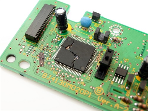
  • If the magic smoke is ever allowed out of the component, the component will no longer function (Figure 1).
  • Much like a can of worms, you can’t put magic smoke back into the component.

Therefore, by the observed effects of magic smoke, you can conclude that it is essential to component operation. Common causes of magic smoke release include (but are not limited to) overvoltage stressing, overcurrent stressing, reversed supply, overheating or incorrect wiring.

Figure 1: The hermetically sealed smoke container is breached, resulting in a component that no longer works

2. You’ll never be alone when you work in isolation. Many electronic systems have multiple different supply “zones.” For example, in a compressor circuit, there will be a high-voltage zone that is several hundred volts to supply power to the motor and a low-voltage zone where the control circuits live and work. To improve the reliability of these systems, designers use a concept called isolation.

Isolation is a way to transport data and power between high- and low-voltage circuits while preventing hazardous or uncontrolled transient current from flowing in between the two. Isolation protects circuits and helps them withstand high-voltage surges that would damage equipment or harm humans – even smart humans like analog engineers. Most sane lab practices require that you not be alone in the lab when working on systems that operate at potentially dangerous high voltages. So if you are working in isolation, grab a buddy and stay safe!

3. Pease isn’t a typo. One of the greatest legends of analog design was the late Bob Pease. He’s credited with developing more than 20 integrated circuits, many of them used for decades in the industry. Bob chronicled his design experiences in a column called “Pease Porridge,” which ran monthly in Electronic Design magazine (Figure 2 shows one of Bob’s quips, signed with his initials, RAP). He also hosted the semiconductor industry’s first online webcast, tailored specifically for analog design engineers.

Figure 2: If you don’t understand the joke, then you need to spend more time in the lab

4. Clocks are no good at telling time. Clocks are possibly the most ironically named analog components because a clock won’t give you the time of day. A “clock” is in reality an oscillator typically used to generate a consistent, stable frequency. Clocks can be a key element of analog design because of interference to and from the clock signal. A clock signal propagating across a board adds noise and accumulates delay. Meanwhile, the clock signal induces noise onto other nets on the board. Clocks can be messy if not done properly, so it is critical that you understand the purpose of oscillators, generators, buffers and jitter cleaners in order to optimize your system.

5. There is a lot of drawing involved for a field this technical. Analog design engineers love to draw. We love to pick up dry erase markers and draw squiggly lines all over a white board. We draw in a language unique to us and undecipherable to the uninitiated (Figure 3). Every major component in a system has its own special symbol, ranging from simple resistors and capacitors up to complicated blocks like analog-to-digital converters (ADCs) and digital-to-analog converters (DACs). These symbols bring meaning and functionality to a circuit long before anything physical is actually made and provide a platform for discussion, starting with the phrase “And this is how it works …”

Figure 3: The secret analog language

6. V = IR is always the answer. It is humorous how useful simple concepts can be. Analog design is home to some very complicated integrated circuits: sigma-delta ADCs, RF amplifiers, digital isolators, etc. Yet the most common design equation is Ohm’s law, a relationship that most people learn in high school or even earlier.

Ohm’s law states that V = IR, or that voltage is equal to current times resistance. Undoubtedly, most of you are rolling your eyes at the fact that I just wasted a whole sentence to describe Ohm’s law, which everyone already knows.

Let’s take a look at some examples of analog design that don’t require a doctorate in mathematics to solve:

  • Current shunt amplifier: A 10mΩ resistor (R) is placed in line with a current up to 10A (I), and the 0-0.1mV (V) is amplified and measured.
  • In a precision DAC, at a 5mA (I) load the output drops by 120mV (V), meaning that the output impedance (resistance) is about 24Ω (R).
  • In a motor gate driver, a MOSFET overcurrent monitor trips at 0.5V (V), meaning that a MOSFET with an on-resistance of 20mΩ (R) has an overcurrent threshold of 25 A (I).

7. Those formulas from Engineering 101 still come in handy today.Moving on from Ohm’s law can be the most jarring event in an analog engineer’s life. While you can solve many problems with V = IR, plenty of designs require more knowhow. From remembering capacitor types, to the equation for discharging a resistor-capacitor (RC) circuit, to calculating noise bandwidth, there can be a lot to keep track of.

Of course no analog designer should wade into these waters alone, so TI put together the Analog Engineer’s Pocket Reference (Figure 4). Reference guides for analog have been around for a long, long time and are a tried-and-true method of giving you all the tips, tricks and facts. I would say that a good reference guide is all you need, but the most critical element to any design is your creativity, ingenuity and excitement for analog.

Figure 4: Some things never change

Are there any more things that only an analog engineer would understand? Comment below and let us know if you have any unique experiences in analog.

“Trust, but verify” SPICE model accuracy, part 5: input offset voltage and open-loop gain

$
0
0

Previous installments of this blog post series discussed the need to verify SPICE model accuracy and how to measure common-mode rejection ratio (CMRR), offset voltage versus common-mode voltage (Vos vs. Vcm), slew rate (SR) and open-loop output impedance (Zo). In part 5, I’ll explain how to verify two of the most impactful specs of precision operational amplifiers (op amps): input Vos and open-loop gain (Aol).

Input offset voltage

Input offset voltage (Vos) is the difference in voltage between an op amp’s two input pins. Typical offset voltages range from millivolts down to nanovolts, depending on the device. Vos adds in series with any externally applied input voltage (Vin), and therefore can cause errors if Vos is significant compared to Vin. For this reason, op amps with low Vos are highly desirable for precision circuits with small input voltages.

Figure 1 shows the application of a 1mV input voltage to an op amp with Vos equal to 0.1mV. Because Vos is 10% of Vin, the offset voltage contributes a 10% error in the overall circuit output. While this is a fairly extreme example, it shows the impact that Vos can have on op amp designs.

Figure 1: Input offset voltage contribution to DC error

To measure the Vos of an op amp, configure the op amp as a unity gain buffer with its noninverting input connected to mid supply (ground in split-supply circuits). Wire a differential voltage probe between the op amp input pins, and make sure to match the power-supply voltage and common-mode voltage conditions given in the op amp data sheet. Figure 2 shows the recommended test circuit.

Figure 2: Input offset voltage test circuit

Let’s use this circuit to measure the Vos of the OPA189, a new zero-drift, low-noise amplifier from TI. Simply run a DC analysis and observe the voltage at probe Vos, as shown in Figure 3.

Figure 3: OPA189 Vos result

The measured input offset voltage is -400nV, or -0.4µV. This correlates exactly with the spec in the OPA189 data sheet.

Open-loop gain

An op amp’s open-loop gain is arguably its most important parameter, affecting nearly all aspects of linear or small-signal operation including gain bandwidth, stability, settling time and even input offset voltage. For this reason, it’s essential to confirm that your op amp SPICE model matches the behavior given in the device’s data sheet. Figure 4 shows the recommended test circuit.

Figure 4: Open loop gain test circuit

This test circuit is very similar to the one used to measure open-loop output impedance. Inductor L1 creates closed-loop feedback at DC while allowing for open-loop AC analysis, and capacitor C1 shorts the inverting input to signal source Vin at AC in order to receive the appropriate AC stimulus.

As explained by Bruce Trump in his classic blog post, “Offset Voltage and Open-Loop Gain – they’re cousins,” you can think of Aol as an offset voltage that changes with DC output voltage. Therefore, to measure Aol, run an AC transfer function over the desired frequency range and plot the magnitude and phase of Vo/Vos. Make sure to match the specified data sheet conditions for power-supply voltage, input common-mode voltage, load resistance and load capacitance.

Let’s use this method to test the Aol of the OPA189.

Figure 5: OPA189 Aol result

In this case, the op amp’s Aol is modeled very closely to the data sheet spec. The spike in the data sheet’s Aol around 200kHz is caused by the chopping network at the input of the amplifier and is not modeled, although its effect on the nearby magnitude and phase response is.

Thanks for reading this fifth installment of the “Trust, but verify” blog series! In the sixth and final installment, I’ll discuss how to measure op amp voltage and current noise. If you have any questions about simulation verification, log in and leave a comment, or visit the TI E2E™ Community Simulation Models forum.

Additional resources

“Trust, but verify” SPICE model accuracy, part 6: voltage noise and current noise

$
0
0

Previous installments of this blog post series discussed the need to verify SPICE model accuracy and how to measure common-mode rejection ratio (CMRR), offset voltage versus common-mode voltage (Vos vs. Vcm), slew rate (SR), open-loop output impedance (Zo), input offset voltage (Vos) and open-loop gain (Aol). In this sixth and final installment, I’ll cover operational amplifier (op amp) noise, including voltage noise and current noise.

Noise is simply an unwanted signal, usually random in nature, that when combined with your desired signal results in an error. All op amps, as well as certain other circuit elements like resistors and diodes, generate some amount of intrinsic – or internal – noise. In analog circuits, it’s critical to confirm that the noise level is low enough to obtain a clear measurement of your desired output signal. Figure 1 shows an example of input voltage, ideal output voltage and output voltage with noise for a circuit with gain of 3V/V.

Figure 1: Noise example

With an accurate model, predicting the noise performance of an op amp circuit becomes quite straightforward. This is very appealing to most engineers, as calculating noise by hand can be cumbersome and difficult.

Input voltage noise density

The voltage noise of an op amp is usually given as input voltage noise density (en) in nanovolts per square root hertz (nV/√Hz), which quantifies how much noise voltage the op amp generates at its input pins for any given frequency. To measure en, configure the op amp as a unity gain buffer with its noninverting input connected to an AC source Vin. Figure 2 shows the recommended test circuit.

 Figure 2: Input voltage noise density test circuit

Let’s use this circuit to measure the en of the OPA1692, a low-noise amplifier from TI. Simply run a noise analysis over the desired frequency range and measure the noise level at node Vnoise with respect to Vin.

In this case, the simulated en matches perfectly with the data-sheet spec, shown in Figure 3.

Figure 3: OPA1692 en result

Input current noise density

Op amps also generate noise currents at their input pins, called input current noise density (in) and typically given in femtoamperes per square root hertz (fA/√Hz). You can measure this in a similar way to en, but you will need to perform a simple trick. Some simulators have trouble measuring noise in terms of current, so a current-controlled voltage source converts the current flowing into the noninverting input pin into a voltage. Figure 4 shows the recommended test circuit.

 Figure 4: Input current noise density test circuit

Let’s use this circuit to measure the in of the OPA1692. Run a noise analysis over the desired frequency range and measure the noise level at node Inoise with respect to Vin. Keep in mind that the resulting plot will have converted amps to volts due to current-controlled voltage source (CCVS1). Figure 5 shows the results after converting back to amperes.

Figure 5: OPA1692 in result

Again, the noise characteristic matches the data-sheet curve extremely well.

Total voltage noise

While knowing the input-referred noise of an op amp is useful, it doesn’t paint a complete picture of your circuit’s overall noise performance. A combination of factors like closed-loop gain, bandwidth and the noise contributions of other circuit elements will affect the total amount of noise that appears at the circuit output. Thankfully, most simulators provide a way to measure this type of noise, called total noise or integrated noise, since it’s the integration of all noise sources over the circuit’s effective bandwidth.

Figure 6 shows a more complex op amp circuit, with the OPA1692 configured for a noninverting gain of 10V/V and an additional resistor-capacitor (RC) filter at the output to limit the effective bandwidth to roughly 150kHz.

 Figure 6: OPA1692 total noise example circuit

Run a total noise analysis over a wide frequency range (shown in Figure 7) and measure the noise level at node Vnoise in order to find the total root mean square (RMS) noise, which will appear at the circuit output. You are looking for the level at which the total noise curve flattens out to a constant value at high frequency.

Figure 7: OPA1692 total noise result

The test result shows that the total noise of the circuit in Figure 6 is equal to 21.15µVrms, or 126.9µVpp. This is what you would expect to measure if you probed the output of this circuit in the real world. However, keep in mind that the random nature of noise means that the actual noise level may be somewhat higher or lower than what you calculated or simulated. For a deeper discussion, watch the TI Precision Labs – Op Amps video series on noise.

Thanks for reading this sixth and final installment of the “Trust, but verify” blog series! I hope you’ve found the information and techniques in this series useful in your pursuit of more accurate SPICE simulations. If you have any questions about simulation verification, log in and leave a comment, or visit the TI E2E™ Community Simulation Models forum.

Additional resources

How to make precision measurements on a nanopower budget, part 1: DC gain in nanopower op amps

$
0
0

Heightened accuracy and speed in an operational amplifier (op amp) has a direct relationship with the magnitude of its power consumption. Decreasing the current consumption decreases the gain bandwidth; conversely, decreasing the offset voltage increases the current consumption.

Many such interactions between op amp electrical characteristics influence one another. With the increasing need for low power consumption in applications like wireless sensing nodes, the Internet of Things (IoT) and building automation, understanding these trade-offs has become vital to ensure optimal end-equipment performance with the lowest possible power consumption. In the first installment of this three-part blog post series, I’ll describe some of the power-to-performance trade-offs of DC gain in precision nanopower op amps.

DC gain

You probably remember from school the classic inverting (Figure 1) and noninverting (Figure 2) gain configurations of op amps.

Figure 1: Inverting op amp

Figure 2: Noninverting op amp

These configurations resulted in inverting and noninverting op amp closed-loop gain equations, Equations 1 and 2, respectively:

where is the closed-loop gain,  is the value of the feedback resistor and  is the value of the resistor from the negative input terminal to signal (inverting) or ground (noninverting).

These equations are a reminder that DC gain is based on resistor ratio, not resistor value. Additionally, the “power” law and Ohm’s law show the relationships between resistor value and power dissipation (Equation 3):

where P is the power consumed by the resistor, V is the voltage drop across the resistor and I is the current through the resistor.

For nanopower gain and voltage divider configurations, Equation 3 tells you that, in order to minimize power dissipation, you need to minimize the current consumption by the resistor. Equation 4 helps you understand the mechanism to do that:

where R is the resistor value.

Using these equations, you can see that you must choose large resistor values that provide both the gain you need while minimizing power dissipation (and therefore power consumption). If you don’t minimize current through the feedback path, you’ll lose the benefit of using nanopower op amps.

Once you’ve determined what resistor values will meet your gain and power-consumption needs, you’ll need to consider some of the other op amp electrical characteristics that will affect the accuracy of signal conditioning. Summing several small systemic errors inherent in nonideal op amps will give you the total offset voltage. The electrical characteristic, , is defined as a finite offset-voltage number between the op amp inputs, and describes these errors at a defined bias point. Please note that it does not describe these errors across all operating conditions. To do that, you must consider the gain error, bias current, voltage noise, common-mode rejection ratio (CMRR), power-supply rejection ratio (PSRR) and drift. Covering all of these parameters is beyond the scope of this post, but let’s look at  and drift – and their influence in nanopower applications – in a bit more detail.

Real-world op amps exhibit  across their input terminals, which can sometimes be a problem in low-frequency (close to DC) precision signal-conditioning applications. In voltage gain configurations, the offset voltage will gain up along with the signal being conditioned, introducing measurement errors. In addition, the magnitude of  can change over both time and temperature (drift). Therefore, in low-frequency applications requiring fairly high-resolution measurements, it’s important to select a precise ( ≤ 1mV) op amp with the lowest possible drift.

Equation 5 calculates the worst-case  over temperature:

Now that I’ve covered theory, including choosing large resistor values to create gain ratios and op amp accuracy for low-frequency applications, I’ll go over a practical example using two-lead electrochemical cells. For two-lead electrochemical cells which often emit very small signals of low frequency, and are used in diverse portable sensing applications like gas detection and blood glucose monitoring, choose a low-frequency (<10kHz) nanopower op amp.

Using oxygen sensing (see Figure 3) as the specific application example, assume that the maximum concentration of the sensor outputs 10mV (converted from current to voltage by a manufacturer-specified load resistor, ) and the full-scale output of the op amp is 1V. Using Equation 2, you can see that needs to be 100, or  needs to be 100 times larger than . Choosing values of 100MΩ and 1MΩ, respectively, gives you a gain of 101, and these resistor values are large enough to limit current and minimize power consumption.

To minimize offset error, the LPV821 zero-drift nanopower op amp is a good choice. Using Equation 5 and assuming an operating temperature range from 0°C to 100°C, the worst-case offset error introduced by this device will be:

Another good choice is the LPV811 precision nanopower op amp. Using its data sheet to gather the necessary values plugged into Equation 5 gives you:

(Note that the LPV811 data sheet does not specify a maximum offset voltage drift limit, so I am using the typical value here.)

If you were to use a general-purpose nanopower op amp like the TLV8541 instead, those values would result in:

(The TLV8541 data sheet also does not specify a maximum offset voltage drift limit, so I again used the typical value here.)

As you can see, the LPV821 op amp is the best choice for this application. With 650nA of current consumption, the LPV821 can sense changes in the output of the oxygen sensor down to 18µV or lower, and introduces a maximum offset gain error of only 2.3mV. When you need both extreme precision and nanopower consumption, a zero-drift nanopower op amp will provide the best possible performance.

Thanks for reading this first installment of the “How to make precision measurements on a nanopower budget” series. In the next installment, I’ll discuss how ultra-precise nanopower op amps can help in current-sensing applications. If you have any questions about precision measurements, log in and leave a comment, or visit the TI E2E™ Community Precision Amplifiers forum.

Additional resources

Viewing all 408 articles
Browse latest View live


<script src="https://jsc.adskeeper.com/r/s/rssing.com.1596347.js" async> </script>