Quantcast
Channel: Analog : operational amplifier
Viewing all 408 articles
Browse latest View live

How to properly terminate an unused op amp

$
0
0

We are often tasked by customers to select the best products to complete a design, including how to configure unused operational amplifiers in quad or dual op amp devices.

While this may seem like a simple question to some, there are subtle aspects of operational amplifier behavior that must be understood to arrive at the correct implementation. In his latest contributed article, analog applications engineer Todd Toporski helps you understand the basics and avoid possible problem scenarios. .

Head over to Electronic Products’ website to read the article on properly terminating an unused op amp, or pick up a copy of the November issue.


Inexpensive analog isolation

$
0
0

Popular applications like LED lighting, brushless motors and power monitoring all require a combination of direct offline power electronics with isolated control electronics. Now more than ever, isolation is necessary in these designs.

An isolated operational amplifier (op amp) is too expensive for most of these high-volume applications. Digital isolation is more cost-effective, but typically requires an analog-to-digital converter (ADC) and multiple digital isolators.

Michael Score, FAE and senior member of TI’s technical staff, discusses a cost-optimized solution for moving analog across the isolation barrier in his newest article. Read it on EDN’s website now, and check out a sneak peek of Michael’s proposed solution in the schematic below. 

Correcting DC errors in high-speed amplifier circuits

$
0
0

When both high DC accuracy and high bandwidth are required at the same time, it may be difficult to implement.  Depending on the circuit configuration, there are several valid approaches including building a composite amplifier, or implementing a servo loop around a high-speed amplifier. 

For an inverting circuit configuration, a DC servo loop using an operational amplifier configured as an integrator is most suited.  For a non-inverting circuit, a DC servo loop circuit based on an operational trans-conductance amplifier (OTA) will be the simplest implementation.  These two circuits are shown below in figure 1 and 2.

Figure 1: DC servo loop for inverting amplifier configuration

Figure 2: DC servo loop for non-inverting amplifier configuration

Both of these circuits are AC-coupled whether you want to use a decoupling capacitance or not.  I represented the circuit here with a decoupling capacitance to emphasize that the equivalent circuit will be AC-coupled. 

The servo loop in effect removes the DC voltage and replaces it with the reference voltage (Vref).  The accuracy of the system is only limited by the accuracy of the device used in the servo loop and the speed of the loop.  In both these circuits, you have to balance the high-pass bandwidth with the response time of the servo amplifier.  If the servo amplifier is too fast or if the change in the signal is too slow, the signal will be servo’ed with disastrous consequences on its integrity.  The system will also have an initial settling time before accurate measurement can be achieved.

For the integrator based circuit, the servo amplifier will see its output voltage increase in direct correlation to the output of the signal amplifier.  The input of the signal amplifier will then be seen at the output as the DC gain is 1-V/V.  The low-pass filter formed by R4 and C3 will limit the bandwidth and minimize the noise contribution to the signal amplifier.  The servo amplifier will normally be a precision amplifier such as the OPA277 or OPA333.

The DC servo loop for the non-inverting configuration behaves the same to the integrator up to the output of the SOTA (sampling OTA) of the OPA615.  The voltage difference between pin 10 and 11 will generate a current output that will charge the Chold capacitor.  The resulting voltage is then fed to another OTA.  The voltage appearing at the B- input (pin 3) of this OTA is mirrored to the E-input as a voltage and converted into a current with the resistor RE.  The current is finally mirrored to the C-output (pin 12) and inserted into the inverting node of the OPA656.  Current will keep adding on to this node until the voltage across pin 10 and 11 is nulled.

Now for some added complexity, the SOTA can be used to sample a specific time, during which there is no signal to achieve a certain DC value, in effect shifting the entire signal up or down.  In this mode, the circuit will behave like a DC-restore circuit.  If the SOTA is always sampling, the DC correction is only achieved by inserting an RC filter on pin 10.  This RC filter will have the same effect as the R4, C3 filter of figure 1.


Decompensated op amps to the rescue

$
0
0

With all the handheld devices at our fingertips these days, from PDA’s and smart phones, to medical devices and test equipment, it’s no surprise we need them to last as long as possible before giving them some juice. 

A key concern, however, is the speed of the op amp since low power usually means limited speed, such as bandwidth and slew rate. I say “usually” because there are exceptions, which we’ll talk about here.

So what do you do if your circuit requires a fairly high gain (20dB or so) but your application can’t really afford all the current needed to boost your speed? This can be a dilemma indeed because we tend to forget about something called decompensated op amps. What benefits can we get from these compared to their unity gain stable counterparts? Simple, we get much better speed. That is, a wider bandwidth and much faster slew rate at no penalty to power consumption.

Bandwidth is expressed as BW=gm/2πCc, where gm is the transconductance and Cc the compensation capacitor. From this formula it’s apparent that the bandwidth is inversely proportional to Cc. Holding gm constant and reducing Cc will surely increase the bandwidth. Does it matter what process we’re talking about? Bipolar, JFET, CMOS? No, the gm of each has different characteristics, but the scheme remains the same.

But what about slew rate? Slew rate is the rate of change of the output over time and is written as SR=dV/dt, which can also be written as I/C. Notice here again the inverse proportionality.

In a decompensated amplifier, there’s no need to boost the current to get either a wide bandwidth or a large slew rate and that’s the primary advantage of these amplifiers. Of course there’s a catch. These are not unity gain stable and will require a minimum gain, usually ten, sometimes five.

To better appreciate the benefits, check out this example:

  • The OPA344 has a unity gain bandwidth of 1MHz and a quiescent current of 250µA max while its decompensated version, the OPA345, offers a 3MHz bandwidth for the same current.
  • Likewise, the LMP7715 offers 17MHz of unity gain bandwidth and a slew rate of about 8V/us for a quiescent current of roughly 1mA. Its decompensated version, the LMP7717, has a bandwidth of 88MHz and a slew rate of 28V/us for a current of….you guessed it, the same 1mA.

The figure below shows the frequency response of the OPA338, a decompensated op amp, compared to the OPA337, its unity gain stable counterpart.

So the next time you’re looking for a wide bandwidth op amp without having to worry too much about power, think of decompensated op amps. They can be very useful in high gain circuits and when used with other precision devices in a composite amplifier fashion.

Engineer it: Thermal considerations when selecting an integrated motor driver

$
0
0
<p>Have you had a chance to watch any <strong>Engineer It</strong> videos yet? We launched this series to bring technical &ldquo;how to&rdquo; design topics to life. Be sure to scroll through the list on <a href="http://focus.ti.com/general/docs/video/Search.tsp?term=engineerit&amp;DCMP=engineerit&amp;HQS=engineerit" target="_blank">ti.com/engineerit</a> to find expert advice that could help with your next design.&nbsp; Looking for guidance on how to select an op amp based on datasheet noise specs? <a href="http://focus.ti.com/general/docs/video/Portal.tsp?lang=en&amp;entryid=1_y7ci5nx4" target="_blank">You&rsquo;ll find a video from amplifiers guru Art Kay there</a>.</p><p><a href="/cfs-file.ashx/__key/communityserver-blogs-components-weblogfiles/00-00-00-03-25/2804.Engineer-It-graphic-for-Analog-Wire.jpg"><img src="/resized-image.ashx/__size/200x0/__key/communityserver-blogs-components-weblogfiles/00-00-00-03-25/2804.Engineer-It-graphic-for-Analog-Wire.jpg" border="0" alt="" /></a></p><p>In this recent video, motor driver expert Mike Firth discusses what thermal specs and characteristics to examine when selecting an integrated motor driver.&nbsp; He outlines the key factors that could lead to overheating: RDSON, switching losses, package characteristics and board layout.</p><p>For advice on selecting an integrated motor driver that will ensure your design can &ldquo;take the heat&rdquo; of the current you&rsquo;re trying to drive, watch the video on thermal considerations now.&nbsp;</p><p><img style="visibility: hidden; width: 0px; height: 0px;" border="0" width="0" height="0" src="http://c.gigcount.com/wildfire/IMP/CXNID=2000002.11NXC/bT*xJmx*PTEzNjMxMTQyNjgwNTImcHQ9MTM2MzExNDI3MDcwMyZwPSZkPSZnPTImbz*yMzc2NDUyMjIxN2Q*YTkyYWVkNGUyZThh/MDg3ZWQ4ZiZvZj*w.gif" /><object name="kaltura_player_1363114266" id="kaltura_player_1363114266" type="application/x-shockwave-flash" allowscriptaccess="always" allownetworking="all" allowfullscreen="true" height="330" width="400" data="http://www.kaltura.com/index.php/kwidget/wid/1_tpzq5vkl/uiconf_id/2342281"><param name="allowScriptAccess" value="always" /><param name="allowNetworking" value="all" /><param name="allowFullScreen" value="true" /><param name="bgcolor" value="#000000" /><param name="movie" value="http://www.kaltura.com/index.php/kwidget/wid/1_tpzq5vkl/uiconf_id/2342281" /><param name="flashVars" value="" /><a href="http://corp.kaltura.com">video platform</a><a href="http://corp.kaltura.com/video_platform/video_management">video management</a><a href="http://corp.kaltura.com/solutions/video_solution">video solutions</a><a href="http://corp.kaltura.com/video_platform/video_publishing">video player</a></object></p><p><i>Can&rsquo;t view the video above? </i><a href="http://focus.ti.com/general/docs/video/Portal.tsp?lang=en&amp;entryid=1_vx0yycs6"><i>Click here</i></a><i>.&nbsp; </i></p>

Noise gain, signal gain, what a pain!

$
0
0

When I was little my grandfather would ask me “what’s heavier, 5 pounds of lead or 5 pounds of feathers?” and I would immediately answer “lead of course!”

Although the volume is not the same, the weight is the same.  When we talk about amplifier noise what do we assume? Signal gain or noise gain? Well it depends, and it matters. It depends on who you talk to because generally people say gain, referring to signal gain, and it matters because your bandwidth is affected by the noise gain. The closed loop bandwidth, or usable bandwidth, is written as GBW/NG regardless of the configuration you’re using (inverting or non-inverting).  For an inverting amplifier, the signal gain is –Rf/Rg whereas for a non-inverting configuration the signal gain is equal to the noise gain, 1+Rf/Rg.

Let’s look at the OPA348, a general purpose 1MHz op amp. Let’s assume the feedback and gain resistors are both equal to 10k. The usable bandwidth in this case is 500kHz or -1MHz/(1+(10k/10k)). The term in the denominator is the noise gain and is the same for inverting and non-inverting configurations. But notice the signal gain in the inverting configuration is –R2/R1 or 1 (magnitude) in this case. The non-inverting DC gain is 1+(R2/R1) and is equal to the noise gain, 2 in our case.

So now your DC gains don’t match and you want to double R2 in the inverting configuration -2(R2/R1) which gives you 2, the same as your non inverting circuit signal gain.

However, the noise gain is now different.  It’s 1+2*(R2/R1), or 3, which means the closed loop bandwidth is 333.33kHz

So the question becomes why would you consider using an amplifier in an inverting configuration? One reason is the benefit of the common mode. The inverting input is at ground (virtual) and you don’t see the modulation you normally would in a non-inverting configuration and you usually get better distortion this way.

You can read more about the importance of CMRR in “Will the real Vos please stand up?” on TI Precisions Design Hub and “What you need to know about CMRR - the operational amplifier (Part 1)” right here on Analog Wire.

                                                  Figure 1

                                                    Figure 2

                                                                 DC gain of figure 1 and 2

                        Increasing the feedback resistor in figure 2 to 20k to match the DC gain of figure 1

What’s the difference between macro models and behavioral models?

$
0
0

Have you ever wondered what the difference is between a Spice macro model and a behavioral model?             

The basic difference is that macro models like the LMV641 are transistor based. There’s of course more to it than that, but before we dive in let’s first talk a little about the history of these models.

A few decades ago there was something called the Boyle model. It was rather simple but nevertheless provided users with the ability to simulate frequency response, look at gain/phase plots, and slew rate and input bias current, but not much else. I said simple because the topology consisted of a differential pair for the input stage followed by diodes, passive elements and some voltage control current sources (or voltage). The output impedance was not modeled properly in these early models and soon the macro was useless if anyone wanted to predict the behavior under specific conditions. How would you know how to compensate your op amp if you don’t know where the pole causing the problem is?

Over the years the Boyle model gave way to full blown macros with usually an input stage, a middle stage often referred to as the gain stage, and a third stage generally consisting of an emitter follower (for bipolar). These models provide users with much more flexibility such as gain dependence on the load (Av=gm*RL), common mode input range, output swing versus load current, offset voltage, CMRR, PSRR and a few more important parameters. However, many lack the proper modeling of the output impedance, which is paramount in any type of stability analysis. What I do like about macro models is the fact that they are easy to read, allowing the user to trouble shoot fairly quickly should an anomaly occur. There are exceptions though and that’s when the model creator decides to purposely “scramble” it.

Behavioral models, such as the OPA320, show you the behavior of the device regardless of the process technology, architecture and topology. They do not use transistors. Just like macro models, these usually address specific parameters such as Vos, Ib, CMVR, Zo, CMRR, quiescent current etc. at a given temperature and voltage. It’s also possible to create models in which datasheet specifications vary with temperature and operating voltage. However, this means a more complex model (whether macro or behavioral) which takes additional time for simulation.

At TI, a dedicated team of talented engineers works closely with the applications team to develop both, macro and behavioral models. Visit the precision amps forum to search for solutions, get help, share knowledge and solve problems with fellow engineers and TI experts.

Read all of Soufiane's blogs here. Don’t miss out on future Analog Wire blogs. Email subscribe using the button at the top, right-hand side of this post.

Let there be light

$
0
0

Converting light into a voltage is no trivial task. Photodiodes are used in various areas ranging from general purpose use, such as automatic faucets, hand dryers and bill counters, to industrial control and optical communication like encoders and optical receivers. Choosing the “right” amplifier depends on the application, but its selection must be carefully tailored to the diode itself.

That’s because the junction capacitance of the diode will form a pole with the feedback resistor of the amplifier to cause a phase lag. Compensating a rather simple configuration, like figure 1, should be a piece of cake right? Hmmm…well it may not be so straight forward.

Figure 1

Remember, the capacitance forming a pole with the op amp feedback resistor isn’t just from the diode. You must also account for parasitics, stray capacitance and the input capacitance of the op amp itself.

Then there’s the question of process differences. Should you pick a bipolar for low noise (voltage noise that is), a CMOS for low input bias current, or a JFET for both as well as low current noise? That choice depends on the sensitivity as well as the circuit components such as resistor values. Even though the input bias can drift quite a bit in a FET input device, it’ll likely do better up to 70ºC A 10pA Ib at 25ºC. The op amp will have just over 200pA at 85ºC which still beats any bipolar input. Remember, that the dark current will also exhibit the same effect (reversed biased diode or photoconductive mode).

For very low levels of currents, where you’ll need a rather large resistor, a JFET is probably a good starting point as it gives a good combination of low noises (voltage and current). One of my favorites is the OPA827.

In applications where offset voltage and drift are important, zero drift amplifiers such as the LMP2021 and OPA333 can be very good candidates. Many people claim that chopper stabilized amplifiers don’t make good transimpedance amplifiers partly because of their higher bias current yet they’re comparable to JFET’s at higher temperature.

In applications such as life sciences and analytical instruments (spectrometry and OTDR), higher speeds are usually needed. In these cases, selectable gain devices such as the OPA857 provide you more flexibility.

One last thing to remember is that decompensated op amps can be useful for your I-V conversion as long as you remember to manipulate the noise gain so that they are stable. For more info on decompensated op amps, check out my blog post called “decompensated op amps to the rescue.”


What you always wanted to know about TINA-TI but were afraid to ask! (Part 2)

$
0
0

In Part 1 I explained how to create a versatile and accurate differential source in TINA-TI which comes in handy when dealing with a fully differential amplifier (FDA) or other differential circuits. In this post, I’ll explain the procedure for importing the model of another device (non TI) into TINA-TI.

Problem: How to simulate your circuit, which may contain non-TI devices, using TINA-TI?

Solution: Import the simulation model of the non-TI devices into TINA-TI and simulate away! Let’s consider a situation you’d need to apply this technique and then work through it.

Learning by Example: You are trying to build a fast (100MHz) MFB 2nd order low pass filter (LPF) which needs a very high speed amplifier. A current feedback amplifier (CFA) is a wise choice given the speed requirement (10x the roll-off frequency rule-of-thumb) so you choose the LMH6703, a 1.2GHz bandwidth CFA. When you simulate or build the circuit you see the classic issue with a CFA where it oscillates with a capacitor in the feedback path, as shown in Figure 1:

Figure 1: A MFP LPF using LMH6703 (CFA) needs modification to function properly

 You could then apply the technique outlined in Expanding the usability of current-feedback-amplifiers application note, which places a ferrite bead (Z) in series with the inverting input (see Figure 2) to:

  • Achieve stability
  • Minimize the noise impact of achieving stability


Figure 2: Stability with minimal noise impact using ferrite bead

To help choose or simulate the right ferrite bead for the application, one could utilize TINA-TI if the ferrite bead manufacturer, such as Lairdtech Ferrite Bead Models zip, provides an electrical simulation model for the device. After choosing a bead candidate, based on its characteristics that fit the LMH6703 stability requirements, follow the steps below to import its model into TINA-TI:

1. Get the zipped beads model, unzip it, and save the unzipped model file (*.lib, many devices combined into one file) to a known directory, such as: “C:\Program Files (x86)\DesignSoft\Tina 9 - TI\SPICELIB”

2. Use TINA’s Tools, New Macro Wizard to import the Pspice model of the new device (i.e. the ferrite chip candidate) as outlined in Figure 3:

Figure 3: New Macro to Point to the right Simulation File

3. Assign a symbol and device pins to the net list, as outlined in Figure 4:

Figure 4: Symbol and Pin Assignment

4. Place the Macro on the schematic as outlined in Figure 5:

Figure 5: Locate and Place New Macro

Now the device is available for simulation on this schematic, and other ones, just like any other built-in model!

If you have chosen the right ferrite bead for the job, running transient analysis should yield a stable transient response (see Figure 6) and little or no frequency response peaking. Noise simulation is also par for the course now that you have a self-contained complete schematic.

Figure 6: Confirm stability with new macro in circuit

Have fun applying this and I look forward to exploring other TINA-TI tips and tricks we will work through together!

Until next time keep your comments and future-topic suggestions coming so that I can gauge the usefulness of this series and respond accordingly and to also guide the direction of future topics for maximum benefit to all.

A new era for CMOS amplifiers

$
0
0

A little over a decade ago, semiconductor design and applications engineers high fived each other when they had working silicon on CMOS because it achieved sub 100uV of input offset voltage in amplifiers with a yield of 80%. Back then, the titans of the industrial space like Allen Bradley, John Deere, Rockwell automation, Siemens and a few others considered CMOS amplifiers for lower cost platforms, but seldom did they choose them for performance.

While bipolar technology is alive and well, new CMOS amplifiers are pushing the boundaries of process limitations with clever design techniques, sophisticated trim methodologies and yield improvements.

Historically, bipolar devices have been on the “preferred” list of engineers for applications requiring high precision. These devices can achieve sub 1uV/ºC of offset drift. CMOS input stages, on the other hand, would yield as much as 5uV/ºC.

The challenge of achieving a very low offset in CMOS input op amps stems from the difference between the threshold voltages (input differential pair) as well as the difference between the gate-source voltage and the threshold voltage (VGS-VTH). Unlike bipolar devices, offset and offset drift are not correlated in CMOS devices whether in weak or strong inversion.

Other challenges in CMOS amplifier design include higher voltage noise flicker and white noise, and generally a much smaller open loop gain which is attributed to a lower transonconductance value compared to that of bipolar input.

One way around the above challenges is to use techniques such as auto zeroing, chopping, or a combination of both, which reduce the offset and the drift greatly (in CMOS) at the expense of more complex circuitry. Chopper stabilized amplifiers provide the lowest drift over extended temperature ranges, but their internal structure puts some limitations on their use.

Another way is to select a very well-trimmed device. To better appreciate the results of such a well-trimmed op amp, check out the newly released OPA192. A true milestone achievement in the design of CMOS amplifiers, this device is capable of rivaling the best available bipolar and JFET technologies.

So the next time you’re in the market for a true precision op amp, take a look the OPA376 if your system requires a low voltage operation, or the OPA192 for higher voltages.

Or, read “Time for a trim?” a blog I wrote on various trim methodologies.

Is it time to move beyond FR4?

$
0
0

Is your circuit board compromising your circuit?  Is it time to consider a change from the standby FR4 board material?  With rising operating frequencies and higher data rates, signal fidelity is more important than ever before.

FR4 has been a mainstay for printed circuit boards for decades now.  I remember one of my first electronic kits. It was a power supply and it did not use FR4.  The kit included a plastic box that had holes on 0.1” centers and the kit was built right onto the box wall.  The kit worked pretty well, but the pass transistor was in a TO-3 package and there was no heat sink.  During use, the pass transistor got hot and melted the plastic on which it was mounted.   Obviously the plastic chosen for this kit was not an appropriate material for the application.  In this case FR4 would have been a far superior choice because of its high temperature performance and glass fiber reinforcement.  In order to assess the suitability of FR4 we should take a quick look at some key characteristics.   Even though mechanical characteristics are very important, I am going to focus on electrical characteristics because this is where FR4 sometimes falls short and it is where the key benefits of newer board materials are found. 

One of the primary functions of a printed circuit board (PCB) is to contain and route signals.  While board geometry is the primary factor in signal containment, the board materials are the dominant factor in signal loss and signal fidelity.  For example, from the Rogers RO4003 datasheet the Rogers dielectric has -0.05dB / inch of loss at 4GHz while FR4 has -0.26dB/ inch.  This is a significant difference in electrical loss. 

Transmission line impedance is determined by geometry, but also by the electrical properties of the transmission line.  Line impedance is directly proportional to the capacitance of the conductor, and the capacitance of a PCB trace is dominated by the dielectric constant of the insulator.  In FR4 the dielectric constant is both larger and more variable.  This means that over process, frequency and temperature, the FR4 trace will have a higher SWR.  High SWR means more loss and more undesired signal radiation as well as inaccurate measurements.  For our LMH6554differential amplifier we used high performance dielectric so that our S parameter measurements are more accurate over a wider range of frequencies. 

Transmission lines are not the only area on a PCB where electrical consistency is critical.  Filters also depend on consistent board properties.  A filter requires good performance both across the pass band as well as the rejection band, meaning that even well beyond the signal bandwidth the board properties are important. 

How to evaluate a transimpedance amplifier (part 2)

$
0
0

In my previous blog on "How to evaluate a transimpedance amplifier, part 1", we looked at the OPA857 performance, but didn’t go in depth in explaining how those measurements were taken.  Now that we’ve have established a reference, let’s work through the implementation.

To summarize, the main challenges to taking measurements with the OPA857 include:

  • Transimpedance configuration
  • Low input capacitance
  • High output impedance

With a 20kW gain and a 1VPP output voltage swing the input current needs to be 50mAPP.  Since the output voltage swing of the OPA857 is class A and the current flowing through a transimpedance is unipolar, the output common-mode voltage will need to be set appropriately.

The current source needs to be low capacitance, less than 1.5pF, to maintain the bandwidth.  The output needs to be high output impedance to control the loading on the OPA857’s output.  Since most of the test equipments we have are 50W  input and output impedance, how do we resolve that problem while not impacting bandwidth, slew rate or distortion performance of the DUT (Device Under Test)?

This leads to individual solution for each measurement type.

The first measurement we will look at is the frequency response, or S21 parameter.  For that we’ll use an HP 8753ES Network analyzer, a 30kHz to 6GHz S Parameter Network Analyzer.  Both input and output are 50W impedance and AC-coupled.  There are two ports in the back of the analyzer that allow controlling the DC voltage on either the input or output.

The two proposed signal chains to measure the OPA857 frequency response include:

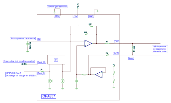
  • Using a high speed differential probe, see figure 1.
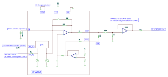
  • Using a high speed buffer to isolate the network analyzer’s load, see figure 2.

Note that the Test_SD pin is set to a logic high (+3.3V) for the internal current source to operate properly.  This implies that the DC voltage present on the Test_IN input will set the output voltage appearing on OUT and requires you implement the following procedure to ensure that the OPA857 operates optimally for an AC response.

  1. Minimize the AC signal.
  2. Set DC voltage at input such that the output voltage can swing around it preset common-mode voltage.  For example, if the signal swing is 500mVPP, then the OUT DC voltage needs to be set to ≤1.4V.  If this is not the case, the output swing will clip as the current in the class-A output stage runs out.
  3. After completion of #1, do not leave anything connected on the output.  A probe lead or a voltage will add several pF to the load, altering the frequency response.
  4. Set the AC amplitude to the desired peak-peak output signal swing.


                               Figure 1: Circuit #1 using a fully differential probe to interface to the HP8753ES.

                  Figure 2: Circuit #2 using a BUF602 to interface to the HP8753ES.

The same approach is used to evaluate pulse response or any time domain measurement.  Note however that since no resistor tolerance inside the OPA857 is better than ±15%, the setup will have to be calibrated device by device.

The approach described above will not work for measuring harmonic distortion, so how does this new problem get resolved?

The traditional approach for measuring harmonic distortion requires:

  • A low distortion source
  • A high dynamic range spectrum analyzer

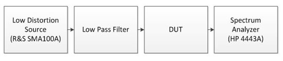
The low distortion source is further improved by using a high order filter.  The dynamic range of the spectrum analyzer can be improved by filtering the fundamental and measuring only the harmonics.  The setup is shown in figure 3.  The notch filter that can is placed after the DUT is omitted in this diagram.

                       Figure 3: Traditional harmonic distortion bench measurement setup.

In the case of the OPA857, we have two problems.  The first one is that the source is a voltage source and that the input signal requires a current source.  The internal current source cannot be used here as it does not have sufficient linearity.  So we will have to develop a low distortion current source to enable the measurement.  The second problem is the interface to the spectrum analyzer.  The output of the OPA857 is pseudo-differential and requires driving a light load, whereas the spectrum analyzer requires a single-ended input and expects 50W.

A current source has high output impedance.  In our case, the current source will need to have low input capacitance as well, so it cannot be generated using transistor-based circuit as a large transistor will also have a high intrinsic capacitance, not considering the package and board layout parasitic.  This limits the approach to using a voltage source and converting it to a current using a resistor.  In order to ensure that the noise gain of the OPA857 is close to 1V/V, the same as the transimpedance configuration, the source capacitance is minimal and the resistance is large enough to approximate this.

The source capacitance is minimized by careful insertion of a series resistor on the inverting pin.  Please refer to the OPA857 EVM for the layout.

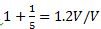
In our case, the gain resistor is five times the value of the transimpedance gain, so for 20kΩ, the current source impedance is 100kΩ.  It is a compromise as the noise gain is  .  This represents a degradation of ~1.6dB due to the loss in loop-gain in the measurement which would not be present in a transimpedance configuration.

The OPA857 is operating in an attenuator configuration, so a 0.5VPP on its output now requires 2.5VPP from the generator further increasing the non-linearity from the source.

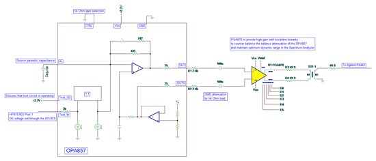
Looking at the output of the OPA857, we need to measure the nominal 500Ω load and also measure the non-linearity of the amplifier as the load is decreased to 5kΩ. So, again the interface between the OPA857 and the spectrum analyzer is not purely resistive as there is too much attenuation of the signal and parasitic capacitance on the output after the resistance would limit the effective bandwidth.  If an active element is inserted in the signal chain, its distortion must be 15dB better than the expected measurement to degrade the measurement by 0.1dB.  This tends to be a relatively easy requirement at low frequency, but is quickly unmanageable as the frequency increases.  The solution here is to use a DVGA developed for the telecommunication market as it provides sufficient gain to compensate for attenuation in the signal path, since those DVGAs have a 200Ω input impedance, as well as convert the pseudo differential signal to fully differential and have sufficient linearity up to the frequency of interest.  A transformer on the output of the DVGA converts the amplified fully differential signal and converts it to the single-ended input the spectrum analyzer expects.  We will have some attenuation losses here as well to match the 50Ω input impedance of the test equipment.  Finally the signal chain on the output of the OPA857 will look like the diagram shown in figure 4.

Figure 4: OPA857 with PGA870 used to adapt the OPA857 load into the Spectrum Analyzer.

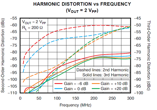
The PGA870 provides additional gain with high linearity minimizing the measured linearity degradation.  Looking into the PGA870 datasheet, we see that operating at high gain (> +10dB), both the 2nd and the 3rd harmonic distortion is greater than 90dBc for a 2VPP output swing.  This ensures that the OPA857 measurement is degraded by less than 0.1dB.

                              Figure 5: PGA870 Harmonic distortion for 200Ω load.

In this blog, I have shown the techniques used to measure most of the typical characteristic curves shown in the OPA857 datasheet.  For application information or how to implement the OPA857, refer to the datasheet and EVM user guide.


What you need to know about using general purpose op amps at low voltage

$
0
0

You need to design a basic op amp circuit at a low supply voltage and are tempted to use that high-voltage, low cost op-amp to save money. But will it work? I’ll show you how to tell.

l started with the LM324 device as my example because it is inexpensive (popular) and says it works down to 3V. The LM2902 supports -40C, and I’ll use this device instead as a personal challenge because cold temperature has the largest voltage diode drops. So, it is the temperature that will cause the most problems with input and output voltage range.

Step 1: Check the valid input and output voltage ranges for the VCC.

The LM2902 doesn’t have 3V parameters, so I’ll use the 5V parameters in figure 1.

Figure 1: 5 V parameters for TI’s LM2902

Input common mode is covered for 5V and higher, but for 3V I am own my own. The rules of electronics still apply at 3V, so I can use the “full range” VICR formula, 0 to Vcc-2V to see my input range is 0V to 1V.

VOH at 25C is pretty simple, VCC-1.5V is 1.5V, but the full temperature range specification is 23V which is VCC-3V for LM2902. That translates down to 0V at VCC=3V… I obviously can’t use that! Looking at the data sheet schematic, I see two VBE drops. Assuming a -2mV/C temperature coefficient, -40C VOH is reduced by 2*(-40C-25C)*-2mV/C=260mV. I’ll round up to 300mV for a little design margin. My new VOH is now VCC-1.5V-0.3V = 1.2V.

VOL is basically 0V for all temperatures, but there is a catch. This only applies for loads terminated to ground. For loads that require the output to sink current, it is a different story. For that, I’ll refer to the sinking current chart in the LM2904-N data sheet (figure 2). It is just as true for the LM2904.

Figure 2: Current sink forLM2904

VOL for moderate current is under 0.8V, but once again this is 25C data and a typical chart too. Looking back at the data sheet schematic, this performance makes sense. And this time, I see just 1VBE for higher current drive. Assuming a -2mV/C temperature coefficient, -40C VOL is increased by (-40C-25C)*-2mV/C = 130mV. I’ll round up to 200mV for design margin. My new VOL is now 0.8V+0.2V = 1.0V

Step 2: Look at the voltage range results and see if I can design anything with them.

Input range is 0V to 1V – this will be a challenge, but I’m OK with it.
Output range is 1.0V to 1.2V – this would be nightmare, I can’t do it.

Step 3: Get creative.

The good news is the output range can be 0V to 1.2V if the output never has to sink current more than a couple micro-amps. The output voltage range can also be increased by using a pull-up or pull-down resistor on the output pin.

A pull-down resistor’s effectiveness on VOL can be determined just by calculating the load driven (be sure to include the feedback networks as loads). The LM2904 will not oppose the resistor for VOL.

A pull-up resistor’s effectiveness on VOH can be determined by calculating the load driven. However the low-current sink (typically 30uA) in the LM2904 will add to the current that the pull-up resistor needs to provide.

So, the LM2902 and other high-voltage low cost op-amps can be used at their stated minimum supply voltage. However load current, load current polarity, input voltage and output voltage must be carefully calculated to avoid design errors.

Extended temperature options

TI’s portfolio of standard logic, power and amplifier functions are now more flexible for industrial designs, with more than 500 devices qualified for extended temperature ranges from –40C to 125C.

 Check out TI’s latest extended temperature logic functions.

Resources:

What you always wanted to know about TINA-TI but were afraid to ask! (Part 3)

$
0
0

Whether or not you were ever “afraid” to ask about any of the TINA-TI topics we discussed in Part 1 or in Part 2 of this Analog Wire series, I’m hoping that you find my next topic, noise analysis using TINA-TI, useful in your day to day work.

Below are some of the TINA-TI noise simulation features which make it a great analysis and optimization tool:

1. Output RMS noise plot over any noise bandwidth.

  • Integration “lower” and “upper” frequencies are entered when noise analysis is initiated.
  • Use cursor(s) to read RMS noise over any bandwidth.

2. Noise density plot- referred to either input or to the output.

  • Input referred noise density, when compared with signal power, lets you observe SNR directly.
  • Output referred density plot to uncover unexpected peaking which could impact noise.

3. Noise gain frequency dependence is automatically factored in.

The requirements for running noise analysis in TINA-TI are listed below:

1. One (and only one) source designed as input. Can be either voltage or current source!  More than one source situation covered below.

2. At least one output node.

3. Active devices macromodels which include noise behavior.

  • Automatically done in TINA-TI when a part is placed on the schematic.
  • Making sure modelled noise matches datasheet is covered below.

4. Start and stop frequency to be specified

  • These entries define the range of noise density x-axis plots but also determine the output RMS noise integration bandwidth.

Figure 1 below shows the noise analysis panel and where the start and stop integration frequencies are entered.

Figure 1: Noise analysis panel & required frequency entries

 Figure 2 shows the use of cursors to find noise over a narrower band. An example of where this may be useful is to see how much noise can be lowered by filtering unwanted bandwidth.

Figure 2: Total noise over any bandwidth using cursors

If your circuit requires the use of multiple sources, simply follow the instructions in Figure 3.

Figure 3: Multiple source strategy for noise simulation

If you doubt how accurate your device noise model is, use the simulation circuits in Figure 4 to generate the plots (Figure 5) which you can then compare with the datasheet:

Figure 4: Uncovering the modelled noise of a device

Figure 5 shows the plots generated by noise-simulating the Figure 4 circuits. Results confirm good agreement with LMH6629 datasheet plots!

Figure 5: LMH6629 TINA-TI noise model matches well with datasheet

In the course of noise analysis, when curious whether the thermal noise (Johnson noise) of any of your resistors is dominant, replace that resistor with Figure 6 circuit (or its Macro provided in link further below). If you find that, as a result, output noise is reduced, then your circuit noise can be improved by lowering that resistor value (and thereby its thermal noise)! This is viable in many amplifier circuits as circuit operation is not affected if resistor ratios are maintained while the resistor values are lowered for lower noise.

Figure 6: Create a noiseless resistor, that you can place on your schematic, to evaluate thermal noise impact

Click here to get the TINA-TI macro using the Figure 6 technique. You can copy and paste this macro in any of your TINA-TI circuits to test for thermal noise (Right click on Macro, select Enter Macro and change “HCCVS1” from 10k to any resistor value you need, as shown in Figure 7):

Figure 7: Noiseless Resistor Macro (how to edit resistor value to what you need)

I’ll wrap this post up by providing a list of suitable devices for your next low noise design. I have included a column in Table 1 called “Critical Resistance” as the value of source resistance beyond which input noise current dominates over input noise voltage. When your source resistance exceeds this critical resistance, it is likely that you can benefit from changing your device to one with a lower noise current. The good thing is that you have TINA-TI at your disposal, to quickly change your device to another type and to run new simulations to verify lower noise.

Device

Voltage Noise

Current Noise

Critical Resistance

see text above

(nV/RtHz)

(pA/RtHz)

(Ω)

Low Voltage Noise:

LMH6629

0.69

2.6

265

LMH6624

0.92

2.3

400

LMH6626

1

1.8

550

LMH6628

2

2

1k

Low Current Noise:

OPA211

1.1

1.7

650

OPA300

3

0.0015

2M

OPA827

4

0.0022

1.8M

OPA657

4.8

0.0013

3.7M

Table 1: Low noise amplifiers

Until we meet again for the next TINA-TI “afraid” series, post your comments here and I will be happy to respond to them.

How to use EMI hardened op amps to reduce your errors

$
0
0

Before the birth of EMI hardened amplifiers, system designers implemented their own filtering scheme. Some worked and others not so well.

A common mishap is to insert a capacitor across the inputs of the amplifier. This approach can cause serious stability issues and usually requires some sort of compensation.

Over the past few years (at least 3), every precision amplifier released by TI  gives customers the peace of mind knowing that these op amps have internal filters which reject any sort of inadvertent RF injected signal into them.

Of course, not all of them reject the same way because the rejection depends on where the cut off frequency is set as with respect to the amplifier bandwidth.

To avoid introducing a phase lag, the IC designer generally picks a cut off that is at least 10x that of the unity gain of the op amp. The order of the filter also determines how much rejection (attenuation) the op amp provides.

As an example 1MHz with a first order filter at 10MHz will reject 40dB at 1GHz. However, a 10MHz with a cut off at 100MHz has a rejection of only 20dB at 1GHz.

EMI errors can have serious consequences on the system. Suppose a 100mV is injected into an amplifier with gain of 100. Let’s say you’re using an op amp with no EMI filters and 30dB of rejection (1GHz). So we have 316mV at the output of the op amp [(100mV/31.6)*100]. Let’s now assume the output is fed to a 12 ADC with a 5V FSR.

Let’s compute the loss of counts caused the injected signal (EMI):

5V/(2^12)=1.22mV, now diving the output of the op amp by 1.22mV (316mV), we see that we lose nearly 260  counts.

Using the OPA172 reduces the count loss to roughly 8. Using the LMV831, which provides 90dB of rejection, reduces it further to 0.25!

So the next time you’re looking for a precision op amp, make TI your first stop and have the peace of mind knowing that all of our latest amplifiers have integrated EMI….at no additional cost!


Check out this clip in our video library for some additional interesting information on How to avoid electromagnetic interference (EMI).


Increasing dynamic performance in radar systems

$
0
0

If you’re designing automotive radar or even commercial or military radar systems, we are all bound by physics.  I’d like to change that, but many of my old professors in college said “there are rules you can bend and then there are laws of nature that are immovable”.  Path loss in radio transmission is one of those things.  So, if you want your radar to see further, you need to improve the dynamic range of your system.

We’ll start with the basics to understand why dynamic range is an issue and where to look to improve it– the radar equation.  This defines how far the radar can see based on various system and atmospheric conditions.  The full (yikes!) equation is shown below (I’m having that math nightmare again!).

But to see the effects on the system, we’ll strip it down to the basics… the classic radar equation.

The first concern is obvious… the range is a function of the ratio of the transmitted power (PS)  including antenna gain and the target cross-section and the minimum power detectable by the receiver (PE[MIN]). This function is the fourth root, so assuming a fixed transmit power and target size while fixing the antenna gain and other constants the equation reduces to that shown below.

Now we see the effect of improving the receiver’s dynamic range and sensitivity.  Improving the receiver’s noise power floor by a factor of 10 db (20 db in voltage noise) theoretically improves the range the radar sees by over 77%.

To fix this, consider the ENOB, or effective number of bits,of the system (not the data converter) that digitizes the returned signal.  There are several things that affect the noise floor such as  clock jitter (a form of noise that affects SINAD), quantization noise (the “bits” of resolution of the converter), and input referred noise of the amplifier chain. 

Let’s start with the digitizer. For most modern radar systems, there is a down conversion stage before the data converters which are often utilized to digitize in the second Nyquist zone.  The ADS4449 is a 250 Msps 14 bit quad ADC with an SFDR of 87 db and a SINAD of over 70 db resulting in an ENOB of 11.5.  This is an excellent choice for many automotive or weather radar applications. 

To get the signal to the data converter we’ll need a low noise mixing stage.  A good local oscillator (LO) synthesizer to consider is the TRF3765 which has extremely low RMS jitter on the order of 350 femtoseconds. To drive the ADC with the maximum dynamic range a high speed, low noise differential amplifier can be used which can utilize the common mode output of the ADC to place the input signal exactly where the ADC requires it. A good choice might be the LMH6552 which is designed to drive modern data converters.

And finally, but extremely important, is a master clock which is often supplied from an FPGA that grabs the output of the ADC. Depending on how far away the clock originates, or how much jitter is present, it’s a good idea to clean it before sending it to the ADC.  Remember, jitter is noise and directly affects the ENOB of the converter, so a clean clock is absolutely essential.  I’d suggest selecting a device from LMK048xx family such as the LMK04808.  These clock cleaners also have extremely low jitter and can restore the master clock as well as distribute the clean clock signals.

So, there you have it.  If you want your radar to see farther, you can use more transmit power, improve your antenna gain or simply use lower noise components in your receiver chain and improve the overall noise performance of the radar’s receiver.

If you’re interested in learning more about SINAD and ENOB, check out my colleague’s blog post called “SINAD, ENOB and the rest of the family”.

… till next time!

What you always wanted to know about TINA-TI but were afraid to ask! (Part 4)

$
0
0

This installment of the TINA-TI series is based on your requests from the list in Part 1. In this post we’ll learn how to generate:

  1. Time varying (piecewise linear) source
  2. Frequency varying source

Time varying source:

In practice, standard waveforms (i.e. square wave, triangular wave, etc.) may not suffice for your simulation and you may need to generate a real-life excitation waveform, similar to what is in your system, to verify bench behavior or to predict performance before you build. For these situations TINA-TI offers the piecewise linear source which can create either transient or repetitive waveforms.

The key to creating the piecewise linear source is to first put the time (x-axis) and voltage, or current (y-axis), in table form (x, y) and then insert it in the TINA-TI source information dialog. TINA-TI does the rest (see Figure 1).

Figure 1: Entering source (VG or IG) information that defines the time-variable waveform

You can even make the waveform repetitive provided one full x-y cycle is defined (see Figure 2)!

Figure 2: Adding simple text commands make the waveform repetitive

As you can see, it is very easy to make a single pulse or a portion of a waveform.

What if the waveform is more complicated, or if you want to use an extensive list of x-y points for more accuracy? What if you like to define the waveform algebraically (using an expression)? Simple!

Generate the x-y table in a spreadsheet program (like Microsoft Excel or equivalent) and copy and paste into the TINA-TI Signal editor panel. Figure 3 is an example of a waveform computed using Excel for a fast exponential rise time and a slow exponential fall time.

Figure 3: Using Excel to compute waveform

Figure 4 shows the resulting repetitive waveform in TINA-TI.

Figure 4: Resulting waveform copied and pasted from Excel

Frequency varying source:                    

TINA-TI has the ability to generate and preform AC Analysis with any waveform / source that is described with a Laplace transform expression involving “s”. This can be powerful in many simulation applications such as filters, electro-mechanical response, Laplace transform magnitude / phase visualization and many others.

Say you are contemplating the characteristics and the order of a filter you need in front of a fully differential amplifier (FDA), such as the 2.8GHz LMH6554, to drive a GSPS analog to digital converter (ADC), like the 12bit 1.6GSPS ADC12J1600, and you’d like to find out the overall response. You know that you will get a “smoother” response from a Butterworth filter, but a Chebyshev filter is bound to have a sharper skirt. If you simulate the response using the filters’ Laplace transforms, and implement your FDA design, you can get the actual response at the ADC input, including any effects from interaction of stages with each other.

You may also include any parasitics in your analysis. Figure 5 is one such example where U1 and U2 TINA-TI macros respectively represent 4th order 100MHz low-pass Butterworth and Chebyshev filters, driving identical LMH6554 single ended to differential amplifiers.  Simulated AC analysis shows the overall transfer function.

Figure 5: Example of AC analysis using frequency variable sources (U1, U2)

The two identical LMH6554 stages used in Figure 5 are so that the two filter type (simulated by U1 and U2) responses can easily be compared side by side and on the same plot. “C_load” included in these simulations is meant to represent any parasitic cap (albeit greatly exaggerated here for emphasis) between the filter output and the FDA input which could affect the response.

Figure 6 shows how one would go about editing the frequency dependent sources (U1, and U2) to tailor these to fit the frequency characteristics we have in mind.

Figure 6: Right click on U1 or U2 macro to enter macro in order to change its characteristics

I hope you enjoyed this installment of the TINA-TI series. I look forward to your comments and questions. The files I used for this post can be found at the very bottom of the blog.

Check out my previous posts in this series to learn more about how TINA-TI can help in your designs. And, for more info on choosing the right filter for your design, check out my colleagues post called “Filter for thought” or the Webench Filter Designer tool.

Minimize your current, pick a sweet spot!

$
0
0

Pick any CMOS or JFET amplifier and you’ll get the lowest possible input bias (Ib) current, right?

Not so fast. If you mean low Ib compared to that of bipolar, then yes. But if you mean sub 10pA, there are other factors to consider. Did you say temperature? Yes, that’s one of the factors, but I was really talking about room temp specs. And one factor you must be aware of is the common mode.

Some of us look at the spec table on the second or third page of the datasheet to determine the value of Ib. Do you look at the top of the page (spec table) where it usually says Vs=5, 10 or 36V and Vcm=Vs/2?

This phenomenon isn’t a design flaw and is due to the leakage of the ESD diodes. As you start shifting from the midpoint, the leakage currents from the diodes fail to cancel each other out. As a result the input bias current increases. How do you get around that? The obvious cure is to operate at the common mode “sweet spot” so that your Ib is at its lowest. What if your application circuit doesn’t allow you to choose the optimum common mode voltage?

No worries, there are a few exceptions. The OPA320 is one amplifier where Ib is pretty flat for about 3V across the Vcm. The LMP7721, another very low current device, uses “special” low leakage diodes with a bootstrap to prevent Ib from rising across the common mode.

The same concept holds true for low power devices. Not Ib but Iq, the quiescent current also varies with the common mode.


So, the next time you’re shopping for a low current op amp, scroll all the way down and check out the Vcm before making a decision.

Thanks for reading! Be sure to leave any questions about what I covered in this post in the comments section below.


SPICE it up: Why I like TINA-TI (Part 1)

$
0
0

TINA-TI is TI’s circuit design and SPICE simulation tool. I’m a big fan of the software, but it’s not just because I work at TI. I’ve used other SPICE-based simulation programs over the years. While most are fairly easy to use and robust, there are several reasons I prefer TINA-TI.

TINA-TI has a simple schematic editor, but it also includes powerful tools, like noise analysis, variance analysis and fast Fourier transform for distortion analysis. An added bonus: it’s free.

But one of the biggest advantages for me as an applications engineer is that TINA-TI has many of TI’s ICs already included and ready to use, including a pre-drawn and linked symbol. When I get a customer support request, I can open TINA-TI, grab the SPICE macromodel for the IC in question and start making initial simulations. This saves me tons of time, and if you’re designing with a new TI device, it’ll do the same for you.

Today, there are more than 650 operational amplifiers pre-loaded into TINA-TI. The software also comes pre-loaded with comparators, fully differential amplifiers, voltage regulators and more – plus a category for other devices. You can often design a whole system with the devices included in TINA-TI

But what happens if you don’t see the device you’re interested in listed in the “SPICE Macros” tab of the software? Don’t worry. Nearly all new TI amplifiers will have a completely assembled TINA-TI reference design available.

To see if a TINA-TI reference design is available for the device, just search for the part number on TI.com and visit the device page, which we call a product folder. Once you get to the device’s product folder, click on the “Tools & software” tab, as shown in Figure 1. You should see links for a macromodel and reference design in the models section. 

Figure 1: Tools & software tab of the LMH5401 product folder

From here, you can download the reference design file, which is a TINA-TI native file format and will automatically open if you have TINA-TI installed on your computer. If you prefer to use your own simulation software, you can also download the macromodel for use in other programs. The reference design will only work in TINA-TI, though.

Once you’ve downloaded the TINA-TI reference design model and have it running, as shown in Figure 2, you can perform a variety of proof-of-concept simulations. 

Figure 2: LMH5401 reference design circuit

For example, I always check DC operating conditions when looking at a circuit. I want to know:

  • Are the power supplies the right voltage? 
  • Are the input voltages in the correct range? 
  • Is the common mode voltage set right? 

A transient simulation will usually show these errors best, but you can also run a “Table of DC results” analysis to start. I usually skip the table and go straight for a transient simulation.

Figure 3 shows the results I got when I ran a transient simulation using the LMH5401 TINA-TI reference design. The LMH5401 is an 8-GHz, ultra-wideband fully differential amplifier (FDA) that can be used in AC- or DC-coupled applications that may require a single-ended-to-differential (SE-DE) conversion when driving an analog-to-digital converter (ADC).

Figure 3: Transient simulation results using the LMH5401 TINA-TI reference design

There are some interesting things going on in Figure 3. For example, why is the signal obvious when the amplifier is off, and why is the input signal impacted so much?

Check back on Friday, Dec. 19, for part 2 in this series, when I’ll answer these questions and walk you through some other helpful simulations.  

Additional resources:

Get Connected: Data aggregation using a general purpose SerDes

$
0
0

Welcome back to the Get Connected blog series here on Analog Wire! In my previous Get Connected blog, we reviewed the benefits of implementing equalization in high-speed serial links that are prone to signal integrity problems. In this post, I will be discussing the concept of using a general-purpose SerDes to aggregate multiple data inputs from different sources for high-speed transmission in short-reach or long-haul applications.

Over time, the need for higher data throughput has grown exponentially, but from a system level the amount of throughput is limited by the physical medium used for data transmission and the high-speed ports that a design supports. For example, if you have to move N Gigabit Ethernet links from one location to another, you are bound by the maximum throughput of a GigE link (1.25Gbps) and the typical transmission distance of 100 meters that Ethernet cabling supports. There are many variants that can be implemented in a GigE design to work around the system-level limitations, but for argument’s sake let’s agree that the parameters above are representative of a typical system.

In order to get your payload from point A to point B, N cables need to be pulled to carry the payload, while point A and point B also need to be within some reasonable distance of each other to avoid data loss. What if you have to transmit your payload across a campus where the distance can exceed one or two kilometers? Solving this problem can be very costly, as cabling is expensive and repeaters may need to be implemented at several points along the bus to deal with signal integrity issues.

TI recently released two general-purpose aggregation devices that deal with such an issue head-on to help reduce overall system complexity and cost. The TLK10022 and the TLK10081 are multi-channel, high-speed SerDes devices that allow for 4 and 8 lanes of low-speed data, respectively, to be aggregated and de-aggregated in the same package to and from one high-speed serial link. The high-speed portion of the SerDes can be configured to support multiple output frequencies, with the maximum throughput being 10Gbps. The low-speed portion of the SerDes can also be configured to operate at many different frequencies and ultimately determines the high-speed output frequency. Figure 1 below depicts a system-level block diagram using the TLK10022:

Figure 1: System-level block diagram using the TLK10022

If we revisit our Gigabit Ethernet example from earlier, it is easy to see that the system complexity and overall system cost is reduced by implementing the TLK10022 aggregation solution. The system cost is reduced dramatically as N cables now become one electrical or optical link, and the system complexity is simplified as N cables are reduced and the need to implement repeaters disappears.

Why stop at Gigabit Ethernet, though? With these devices, the aggregation style in the system makes it possible to aggregate any type of data within the bandwidth limitations of the device. The first aggregation style would be applicable in Ethernet applications: byte interleave mode. In this mode, the aggregation device is looking for 8b10b encoded data on its low-speed inputs. The aggregation core takes the 10-bit words and multiplexing the signals out of the high-speed portion of the IC. The second option for aggregation is bit interleave mode. In this mode, the device works in a round-robin format, taking 1 bit at a time off of each of the low-speed lanes, while again multiplexing the signals out of the high-speed portion if the IC. There is no pre-processing of the data with the aggregation device, it simply multiplexes the incoming data out of the high-speed portion of the IC at an aggregate faster speed. The receiving de-aggregation device is configured in the same manner as the aggregation device, making the data transfer complete.

Recently, the TLK10022 was demonstrated at the electronica trade fair in Munich, Germany. In this demo, the TLK10022 was used to aggregate and de-aggregate four HD-SDI signals running at 1.485Gbps. The four signals were aggregated into a 5.94Gbps optical link, then de-aggregated and shown on four independent monitors. This demo showcased the power and versatility behind TI’s aggregation technology. Watch a video about the demo here. Figure 2 below also shows an image of this HD-SDI demo from electronica. 

Figure 2: Gigabit video aggregation

For more information on specific aggregation application solutions, please visit the High Speed Interface Forum in the TI E2E™ Community to check out existing posts from engineers already using TI interface products or create a new thread to address your specific application. If you are not connected, you can get connected with one of the broadest interface portfolios in the industry.

Please watch for my next post in the Get Connected series, where we will discuss using differential transceivers in unconventional applications. Leave your comments in the section below if you’d like to hear more about anything mentioned in this post or if there is an interface topic you'd like to see us tackle in the future!

And be sure to check out the full Get Connected series!


Viewing all 408 articles
Browse latest View live


<script src="https://jsc.adskeeper.com/r/s/rssing.com.1596347.js" async> </script>