Quantcast
Channel: Analog : operational amplifier
Viewing all 408 articles
Browse latest View live

SPICE it up: My favorite “proof-of-concept” simulations (Part 2)

$
0
0

In my last post, I explained what TINA-TI is and introduced how to use a transient simulation to check a circuit’s DC operating condition. Figure 1 shows the results of this simulation.  

Figure 1: Transient simulation results using the LMH5401 TINA-TI reference design

As an applications engineer, this simulation is one of my favorites, because it tells me if the:

  • Power supplies are the right voltage.
  • Input voltage is in the correct range. 
  • Common mode voltage is set right.  

When these three conditions are set correctly, the output signal will be uniform and not distorted. As shown in Figure 1 above, we can see that the VIN signal is centered on the proper input common mode voltage of 2.5V. The output voltage is the proper amplitude as well. So these conditions look good, but adding another probe, as shown in Figure 2, will help to confirm that everything is set up right. More on that later.

Figure 1 also shows the PD chart on the top row. The power pin is toggled, and the amplifier is turned on and off. Why is the signal obvious when the amplifier is off?  And, why is the input signal impacted so much? 

The output signal that is visible during the “off” time is the feed-through caused by the feedback resistor network. This is why nearly all fully differential amplifiers (FDAs) are not suitable for multiplexing; they are never really “off.” 
The input signal is changing due to the change of input termination. The 8-GHz, ultra-wideband LMH5401, like most FDAs, has active termination when driven from a single-ended source. This means that the input impedance, as seen by the driving source, is set by the amplifier’s closed loop gain. Since the amplifier does not operate during power down, the loop gain is gone, and all that is left is the passive feedback network. As a side note, this active termination allows much lower input noise. 

Now let’s take a look at a transient response. But before we can do that, we should add some more probe points.

The VOUT waveform is OK for starters, but it has no DC information (it is differential only). By adding a probe on one of the amplifier output pins that is referenced to ground, we can see the DC level of the amplifier outputs. Since the output signals on the amplifier output pins are designed to be symmetrical, we only need one probe. This is shown in Figure 2 as the VF1 probe, which is ground referenced.

In Figure 2, I also moved the VIN probe to look at the amplifier input pin (INN). This will enable us to make sure the amplifier input range is valid. Notice that this probe is also ground referenced. 

Figure 2: LMH5401 schematic with additional probes.

In the results shown in Figure 3, the voltage range of VF1 is from 1.97V to 3.0V. This is within the datasheet swing values of 3.9V and 1.1V. Likewise, the input voltage is between 2.31V and 2.65V. This compares to the valid range of 0V to 3.8V. 

Figure 3: LMH5401 transient response with additional probe information shown

Now that we’ve verified that the amplifier operating voltages are well within the range of the amplifier, what else should we simulate?

The next thing I usually check is the AC response. The AC transfer characteristic simulation does not require any circuit changes. It substitutes a small-signal, swept source for VG1 automatically. Figure 4 shows these results.

Figure 4: LMH5401 AC, small-signal response

Everything here looks good. The PD chart is not relevant, so we can ignore it. VF1 (-1.03dB) is the response of one output, and VOUT is the differential response (5.15dB). The difference between VF1 and VOUT is very close to the expected 6.02dB (remember, we are looking at voltages, not power). 

On the VIN chart, note how the input voltage increases at high frequency. This is because the loop gain of the amplifier is reduced, and the active termination, which I mentioned above, becomes less effective. The amplifier gain increases along with the input impedance, which causes less loss in the source resistance (R1).  The only drawback to this behavior is that the amplifier noise increases. Just run the noise analysis in TINA-TI to prove this.

While there are many simulation tools out there, be sure to pick one that will allow you to quickly and easily find the data you’re looking for, like TINA-TI.

The high-speed amplifier applications team has fielded a lot of questions about how to use TINA-TI in the High Speed Amplifier Forum. Check out our answers, and if you have a question that hasn’t been answered, I hope you’ll let us know by posting. We’re here to help.

Additional resources:


JESD204B: What is deterministic latency? Why do I need it? How do I achieve it?

$
0
0

What is deterministic latency?

As I discussed in my last two blog posts, JESD204B: Understanding subclasses: Part 1 and Part 2, the JESD204B data converter interface standard provides two subclasses to achieve deterministic latency: subclass 1 and subclass 2. Most who are familiar with the standard would agree that the deterministic latency feature of JESD204B is one of the standard’s key advantages. But what is it? Why is it so important?

A deterministic system is one where no random processes are involved in the formation of a system’s future states. Therefore, given the same initial conditions, the final outcome will be the same every time.

Latency is defined as the time it takes to go from point A to point B. In a JESD204B link, latency occurs from the input to the TX block to the output of the RX block. This is called link latency, as shown in Figure 1. 

Figure 1. Block diagram of simplified latencies in a TX-RX JESD204B link. Deterministic link latency is achieved by using the elastic buffer with an appropriate data release point.

By definition, achieving deterministic link latency for a system means that the system will be able to have a fixed link latency from startup to system startup. You can calculate the total latency by adding the data converter latency (normally specified in the data sheet) with the deterministic link latency.

Why is deterministic latency important?

So why is it important to achieve deterministic latency? Some systems, such as feedback loops for digital pre-distortion and automatic gain control loops, are sensitive to latency variations, while other systems, such as defensive countermeasures used in military applications, are sensitive to total latency. Also, any system that requires multi-device synchronization, such as phased-array radars, beam-forming antennas or medical imaging equipment, will need to achieve a known, fixed deterministic latency for all devices to achieve synchronization.

How do you achieve deterministic latency using JESD204B?

There are two requirements to achieve deterministic latency from startup to startup:

  1. Alignment of all local multi-frame clocks (LMFCs) at the TX and RX devices
  2. Release point for the data set to after the latest arriving lane

To achieve alignment of all LMFCs at the TX and RX devices, you will need to reset and align the LMFCs using subclass 1 (SYSREF) or subclass 2 (SYNC), as provided by the standard and discussed in a previous blog post. The aligned LMFCs establish a common time reference and provide a fixed-phase offset for each of the devices.

Typically all of the lanes of a JESD204B link are buffered and aligned so they are released together at the next LMFC data release point. In most cases, this ensures the system is deterministic. However, there are cases where the total link delay for the lanes is very close to the LMFC edge, and with some system variations, the last lane may arrive after the LMFC edge. This would force all of the lanes to release at the next LMFC edge, which results in a latency that may vary by as much as 1 LMFC period and is not deterministic from startup to startup.

Figure 2. A non-deterministic latency case. Variations in the arrival time of the last lane may span past the LMFC edge, and the data release point may be off by as much as 1 LMFC period from startup to start up.

You can fix this problem by using the elastic buffer in the JESD204B receiver block. The release buffer delay (RBD) setting controls the elastic buffer and allows the user to select and set the number of frames (1 to K frames) after the LMFC edge as the data release point.

To do that, you must first calculate the maximum link latency, including possible variations across process, voltage and temperature. If there is enough margin away from the next LMFC edge, you can set RBD to K, which will release all of the aligned lanes on the next LMFC edge.

With system variations, the lane arrivals may span over the LMFC edge that defines the data release point. In this case, some number of frames may be chosen with the RBD setting to set the data release point to occur after the uncertainty of the arrival of the lanes. You can use the RBD setting to set the data release point to minimize latency or to provide more margin from the uncertainty caused by variations in the system.

Figure 3. Using RBD to set the release point later than LMFC to account for system variation guarantees the same latency in both cases.

The ability to delay the release of data to account for delays caused by system variations guarantees deterministic latency from startup to startup and over process, voltage and temperature.

Stay tuned for my blog post next month, which will explain how to calculate the expected link latency.

Additional resources:

Interface with TI at CES

$
0
0

It’s the beginning of the year, and that means another Consumer Electronics Show is upon us! You may or may not know it, but TI will be in attendance this year, set up just off the main show floor in the North Hall, ready to show the latest and greatest innovations. Typically, you hear big news announcements from OEMs announcing cutting-edge audio and visual devices and, in recent years, from wearable manufacturers, who are increasing their presence in a big way. Regardless of what electronics you are into, though, TI is usually in it.

When it comes to consumer electronics, we got your back…the back of your TV, that is. This year, we will showcase demos for our HDMI 2.0 retimer. HDMI 2.0 will enable almost double the speed of HDMI 1.0, reaching up to 6 Gbps! Our new retimer will keep that data on track, making sure you can get higher quality content without any hiccups or lag. Along the same pluggable line, we will also have demos for what’s sure to be a hot topic this year: USB Type C. This universal plug will fend off the minor offences of Murphy’s Law by removing the opportunity to insert the “wrong side” for the USB plug first. You will see these universal plugs being added this or next year in tablets and PCs first, but soon it will proliferate in the broader consumer world and hopefully even into automotive spaces.

Speaking of automotive, infotainment is getting a big upgrade this year with easier integration of your phone to your main console. The backbone of this communication system is driven by USB host and on-the-go, which has resurged in recent years. It enables your smartphone to become the controller instead of just another accessory “on the bus.” You probably heard about some of the OEM level software solutions for these applications but if you happen to get into the TI booth you can actually see our seamless solution in action. It’s finally an elegant way to allow your phone be your own personal entertainment director for the duration of your journey, be it to get some more milk from the store or see your grandparents across the country.  

Amid all the excitement that comes from the latest and greatest announcements, take a moment to reach out to your TI rep and make an appointment to stop by to see the innovation that’s going on under the hood at TI’s booth at N115-N118. If you aren't in Vegas this year you can always check out our latest solutions at ti.com/USB. Either in person or on the web, it’s your opportunity to get a peek at the building blocks for next the CES gadget du jour.

Timing is Everything: Understanding LVPECL and a newer LVPECL-like output driver

Replacing multiple devices with one? That’s good logic.

$
0
0
Logic ICs are handy devices engineers sprinkle in for quick translation fixes in their designs. However, simple fixes along the way sometimes complicate things even more. There are many reasons why an engineer would choose to use a logic device in their application. (read more)

JESD204B: How to calculate your deterministic latency

$
0
0

In my previous blog, I explained how to achieve deterministic latency by aligning the LMFC signals at the transmit (TX) and receive (RX) devices and using the release buffer delay (RBD) to set the data release point to follow the expected arrival of the latest arriving lane. In this post, I will show you how to calculate the expected link latency using device parameters of the TX and RX devices.

Total latency is the sum of the analog-to-digital converter (ADC) core latency plus the link latency. ADC core latency can usually be found in the ADC datasheet. Link latency is defined as the time when samples enter the TX serializer, traverse the SERDES lanes, go through the RX de-serializer and come out of the elastic buffer. This is shown in figure 1.

Figure 1. Summary of the total latency from signal input to parallel out (S2PO). It is comprised of the ADC core latency and the JESD204B link latency. You can adjust the elastic buffer to optimize link latency.

You can calculate the link latency using the following information, which should be available from the TX and RX device vendor:

  • Determine the alignment of the TX and RX local multi-frame clock (LMFC) with respect to the arrival of SYSREF (subclass 1). Any offset between the TX and RX LMFC will be accounted for as a fixed delay. The device datasheet for the TX and RX typically provides this parameter as some number of frame clock cycles. The difference is given by tRX_LMFC-tTX_LMFC.
  • Calculate the expected link delay accounting for system variations. The link delay starts at the TX LMFC edge and ends at the RX de-serializer output. The link delay is the sum of the TX serializer delay  tTX SER, the lane delay tlane and the RX de-serializer delay tRX SER.
  • Choose the elastic buffer release point that provides margin against delay variations. Typically, the elastic buffer release point is set at the next LMFC edge following the arrival of the last lane. In this case, the RBD is set by default to K frames (1 MultiFrame) from the prior LMFC edge. This causes the data to release at the next LMFC edge following the arrival of the last lane. However, if all the lanes, including system variations, arrive at some point in between LMFC boundaries, the RBD can be set less than K to optimize the link latency.

Figure 2. Link latency starts from the TX LMFC to when the data is released from the Elastic buffer. RBK<K can be used to optimize the link latency.

Once you’ve done this, you can calculate the link latency as the composite of the delays from the TX LMFC edge when the data enters the TX serializer to when the data comes out of the Elastic buffer. This includes the difference between the device TX-RX LMFC edges, some integer number of multi-frames spanning the link delay and the RBD number of frames in the elastic buffer. The total latency would then be the fixed ADC core latency + the link latency.  This can be expressed as a function of the frame cycle in the following equations:

N = Minimum integer number of whole RX multi-frames spanning the link delay

K = Number of frames in a multi-Frame

RBD = Number of frames in the elastic buffer, worse case latency assume RBD=K

You can determine parameter N by meeting the requirements of the following equation, which states that the link delay (TX serializer delay + lane delay + RX serializer delay) minus the TX-RX delay must fit within the time span of N whole RX multi-frames + RBD frames of the elastic buffer:

As an example, let’s look at Figure 3, which gives the parameters for the LM97937 ADC and Kintex 7 FPGA with K=32.

Figure 3. Example link delay parameters for the LM97937 and Kintex 7 FPGA

For RBD set less than K (assume RBD=24), Eq.3 results in the following inequality: 

The minimum integer solution is given by N=2 and the resulting the link Latency (Eq.1) and total latency (Eq.2) would be:

Check back in February for my next blog post, which will examine how to choose the RBD value and a method to measure and verify the calculated total latency.

Additional resources:

Consumer electronics benefit from analog technology

$
0
0

As we look back on another CES in Las Vegas, it continues to amaze me how much of these consumer electronics contain large amounts of analog. Without the analog functions, consumers would have no idea how much talk time is left in their cell phones, be able to listen to music, take fantastic photos or many other common functions of today’s consumer devices. I guess I’m a bit biased (being an analog guy), and I do recognize the extreme value provided by processors and other digital components, but without the ability to move between the real world and the digital domain, many consumer devices wouldn’t exist.

One area that remains squarely in the analog domain is sensors – the bridge between our physical world and the digital engines that drive these devices. Just about every consumer device has a sensor of some sort, from simple temperature sensors to elaborate multi-sensor systems utilizing sensor fusion to augment reality.

One new breed of sensor that is finding its way into personal electronics is inductive sensing. Inductive sensing has been used in industrial control for years, but with fully integrated solutions, such as the LDC1000, consumer products like cameras, domestic robots and more can greatly benefit from accurate positioning and proximity measurements. A good example of this is an auto-focus lens. Using inductive sensing as a positioning sensor is extremely simple and accurate – so the processor always knows what the current setting is on the lens.

Other sensors can be extremely beneficial for the healthcare sector. There are a number of new personal fitness and home health monitors that utilize acceleration to measure steps and activity, as well as skin resistance and pulse oximetry to measure sweat levels and blood oxygen content. Check out this video on the heath/fitness area at CES.

Devices like the AFE4400 use a simple photodiode and a couple of LEDs to create an entire analog front-end for measuring blood oxygen content as well as pulse rate – all in a tiny package taking up little more space than the bottom of a pencil eraser. These devices are very low power, allowing them to be used in portable applications ranging from in-home medical monitoring to wearable fitness devices. If you are anything like me, having digital personal trainers bugging you to work out is helping to keep those new year’s resolutions!

Personal electronics like smart phones, DVD players and HDTVs all rely on audio amplifiers. Their function has evolved to be extremely efficient using switched-mode amplifiers that use very little power, but provide excellent fidelity. Highly integrated devices such as the TAS5760LD provide a complete solution that converts a digital audio stream (via an I2S interface) directly to speakers. It even has a sophisticated headphone driver for consumers who want to listen in private – all this in a tiny 48-pin TSSOP package.

The future of consumer analog is extremely bright with new sensor technology and highly integrated, low-power analog chips, enabling all kinds of new devices. So next year when you’re walking around CES or simply reading the reviews of all the new gadgets, remember that most of them would not be possible without the analog. Till next time…

How to eliminate a power supply when using a fully differential amplifier

$
0
0

There’s a common misconception when designing with a fully differential amplifier (FDA). Designers often convert a single-ended bipolar signal into a differential signal with a DC offset to drive an analog-to-digital converter (ADC) with a single positive supply in a configuration similar to the one shown in Figure 1.    

Figure 1: FDA driving an ADC

In this example, a single-ended +/-1V signal is converted to a differential signal with a gain of -2 and shifted up by 1.5V to drive an ADC with a single supply.

The misconception is that the FDA must have a symmetrical negative supply since its input is symmetrical with respect to ground. However, if the FDA can accept inputs as low as its negative supply, the symmetrical negative supply is unnecessary. You can actually use the board ground as the FDA’s negative supply, as illustrated in Figure 2. 

Figure 2: Typical FDA circuit performing the single-ended-to-differential conversion

With the negative FDA supply at ground, the FDA’s negative ouput, Vout_neg, can never be below ground. Since the positive input of the FDA, Vin_pos, is just Vout_neg attenuated by Rg/(Rg+Rf), Vin_pos can never be below ground. The high open-loop gain of the FDA creates a virtual short between the two inputs, which ensures that the FDA’s negative input, Vin_neg, is never below ground.

Even if the input signal is pseudo-differential and referenced to a negative voltage, you may still be able to use ground as the negative supply of the FDA. In Figure 3, assume that Vref = -0.1V, minimum Vout from the FDA data sheet is 0.2V, and Rf = 2Rg for a gain of -2:

Figure 3: FDA with a pseudo-differential input

The equation for the minimum input on the FDA positive input, Vin_pos, is as follows:


The virtual short at the FDA inputs ensures the inputs of the FDA will never be below ground.

If you set the FDA gain and Vocm so that the minimum Vout_neg is higher than the value specified in the FDA data sheet as the minimum output, even lower values of Vref may be acceptable.

The bottom line is that an FDA with negative-rail inputs (NRI) can save the expense and board space of a negative FDA power supply when converting a single-ended or pseudo-differential signal into a differential signal with positive offset. Be sure to look for a single FDA supply between 3V and 5V and consider a high-bandwidth, low-power FDA, like the THS4521.

Additional resources:


Make signal conditioning easy with WEBENCH® Interface Designer

$
0
0

Both at home and at work, we are becoming increasingly accustomed to conveniences like high-definition video streaming, millisecond financial transactions and on-demand software as a service (SaaS). To support the ballooning requirement for higher rates of data transfer, the modern-day data center has been quietly on the forefront of high-tech innovation.

A field that began rather humbly, focusing on megabits-per-second data transfer, is now a complex and vibrant ecosystem of mechanical and electrical standards for storage and networking, ranging from 1 Gbps to 100 Gbps. Yet while data centers continue to push technical boundaries each year, it is still normal to hear phrases like “black magic” and “voodoo” used in high-speed design centers.

Hardware designers implementing high-speed interfaces in their storage and networking enterprise systems often rely on sophisticated, expensive design tools to increase their confidence in new chassis designs before proceeding to hardware fabrication. However, system designers lack an easy-to-use tool that can help them narrow down their solutions before beginning more intensive system simulations. In the absence of a simplified simulation tool, system modeling can become complex and prohibitive for smaller businesses or “white box” server vendors (unbranded servers offered by contract manufacturers). To simplify and accelerate the product selection and validation process for every customer, TI has released a groundbreaking new high-speed simulation tool—WEBENCH® Interface Designer.

WEBENCH Interface Designer is a free, browser-based interface design and simulation tool that enables designers to:

  • Visualize their high-speed link by selecting TI interface ICs and custom channel properties to model their system
  • Analyze the electrical performance and specification compliance of their links by using a built-in, Input/Output Buffer Information Specification (IBIS) Algorithmic Modeling Interface (AMI) standard-compliant signal integrity analysis engine
  • Optimize their design by leveraging the full configurability of IBIS AMI models and a real-time eye diagram plot for quick iteration. Link optimization is a unique capability of this tool, reducing iterations when trying to find the optimal design parameters.

Industry professionals will have an opportunity to see Interface Designer live at DesignCon 2015, booth #817, where TI and FCI will be demonstrating an Interface Designer simulation side by side with real hardware, leveraging TI’s DS125BR820 multiprotocol redriver and FCI’s AirMax VS2™ connector. TI is also pushing the boundaries of data center innovation, demonstrating 25 Gbps signal conditioning with FCI (booth #817) and TE Connectivity (booth # 743). For more product information, see www.ti.com/sigcon.

To test Interface Designer for yourself, go to ti.com/webenchinterface and push some boundaries of your own.

Additional resources:

CAN bus arbitration: To yell and back

$
0
0

In the real world, if two people speak at the same time, how do you determine who should speak? Sometimes it’s the one who talks the loudest, and that’s essentially how a controller area network (CAN) bus works.

In a CAN bus, all transceivers transmit the priority of their message (from LSB to MSB); the highest-priority message gets to be transmitted. Specifically for CAN, if two transceivers transmit at the same time, they both are “opening their mouths” to transmit a “0” (logic high); the lower the number, the more important the message. In other words, if two transceivers are “yelling,” the first to “close their mouth” has to wait until the other transceiver finishes transmitting. This whole process is called arbitration (nondestructive arbitration to be exact), which is also what I call any conversation with my father-in-law.

A plethora of robust languages are at your disposal when designing a communications system. Some of them are more mature and well-defined while others are still evolving, such as the CAN bus. CAN is a very robust differential signaling communication protocol. It was originally designed for automotive applications to allow microcontrollers, sensors or other integrated circuits to communicate without the need for a host controller.

The principals of CAN operation make it very robust as well. Its differential signaling topology makes it very resilient to coupled noise. This allows the transmission lines, CANL and CANH, to stay together if there are shifts caused by noise in ground planes. Unlike other differential protocols when CAN is in a recessive state (a logic 1), both lines will rest at the same voltage, typically VCC/2  (unless there is a 3V CAN bus transceiver, which is another conversation entirely).  When the CAN lines are driven apart this becomes a dominant state and a logic 0. Think of the CANL and CANH lines as lips of a mouth: L is your lower lip and H is your upper lip. When you want to communicate, you assert yourself by separating your lips and opening your mouth. This is active low logic signaling, where a “0” is asserted by you speaking. When you are not speaking, your lips are shut tight, causing your CANH and CANL lines to rest together at VCC/2.

Figure 1: CAN signaling and logic levels

Beyond the fundamentals, the CAN bus is evolving. New tweaks and enhanced functionality are making the technology more efficient and unlocking new levels of performance. One of the more recent additions is the idea behind flexible data rates, or FD.

This is lesson No. 1 on how to speak proper “CAN.” You can find out more about CAN FD and our products in a previous blog post, “The need for even more speed: CAN FD.” For the latest and greatest products TI has to offer, check out http://www.ti.com/lsds/ti/interface/can-overview.page.

Additional resources:

Precise industrial data acquisition: The heart of the matter

$
0
0

The primary function of nearly every industrial application of electronics is to perform some sort of operation or function (usually with an embedded processor) based on the value of a physical “real world” analog signal. For the embedded processor to do its job, the analog signal must first be converted from analog to digital. Acquiring and converting the analog signal so that its digital representation is as close as possible to the original analog value fundamentally drives the accuracy of the measurement you can achieve and ultimately the performance of your industrial system. This is why data acquisition, or DAQ, is one of the most important subsystems of industrial electronic systems, and the analog-to-digital converter (ADC) is at the heart of the DAQ subsystem. 

Although to us most are hidden in plain sight, industrial systems play an integral role in nearly everyone’s day-to-day activities. For example, take a ride on an elevator. When the doors open, is the elevator perfectly aligned with the building floor? It’s all about the fine-grained accuracy of the motor position, measured by a high-resolution ADC in a DAQ subsystem from an optical analog motor encoder. In modern parts of today’s world, reliable electricity is so ubiquitous that we can easily take it for granted. However, there are industrial electronic systems monitoring the quality of delivered power by constantly measuring voltage and current being delivered to ensure safety and optimal power delivery. The heart of this again is an ADC. Consider an automated production line and all of the sensing complexities such as position, level, temperature and pressure. All of these measurements need to be obtained from various sources, with different electrical requirements, and done so efficiently. This can be easily done with a multi-channel ADC.

If the ADC is the heart of the data acquisition subsystem, the drive signal conditioning that interfaces to the ADC is the coronary artery. It is important to take great care in the design of the input and voltage reference drive signal, to ensure that the ADC’s performance is in top shape and uncompromised by inferior driving circuitry design. See this TI video for a thorough example of how to select an op amp to drive your SAR ADC. It walks you through the steps to design an ADC DAQ signal chain, including theory, calculation, simulation and verification using the ADCpro software.

Thoughtful selection of ADC, op amp and reference drive circuitry will promote a healthy heart in your design and precise data acquisition in your industrial system.

Additional resources:

Solving the problems of mechanical buttons and capacitive touch sensors

$
0
0

Have you ever had a button that gets stuck when you press it? Or how about one that won’t go down because something has fallen between the air gaps?

While mechanical buttons can be an inexpensive option for your design, they can sometimes have problems. To solve this, a capacitive touch interface has been incorporated into a vast number of products. However, those can have issues of their own. Have you tried to use these products with gloves or in a noisy area where you can’t hear it register? What about when there are contaminants on the surface?

In order to solve both of these problems simultaneously, we need to look at the pros and cons of both of these types of buttons.

InterfaceProsCons
Mechanical Button
  • User can feel the click of a button press
  • Immune to various environmental conditions
  • Reliability concerns due to physically moving parts
  • Cleanliness issues
Capacitive Touch
  • No button gaps
  • Easily cleanable
  • Input design can be more flexible, variable and clearly labeled
  • User cannot feel the click of a button press
  • Susceptible to issues when exposed to the environment 

These pros and cons can be broken into essentially two categories: feeling the press of a button and press detection reliability.

Feeling the press of a button:

As you may have noticed, the newest smart watches do not have mechanical buttons but instead have users tap to receive a haptic feedback response. This haptic feedback is accomplished with an actuator inside the device. When the device detects a press, the device will simulate the feeling of pressing a button by driving the actuator with a certain acceleration profile that mimics a button press or tap. A number of products, including smartphones, wearables and automotive infotainment equipment, already use haptics to provide a better user experience. A general guide to choosing an actuator for these kinds of applications can be found here.

Press detection reliability:

The best feature of a mechanical button is that it uses displacement to detect button presses. However, that movement is also the factor that causes reliability and cleanliness issues. Although capacitive touch increases reliability by not having mechanical movement this technology can have noise issues when exposed to the environment. To solve this problem, a system that can detect mechanical displacement but doesn’t “really” move is needed. TI has come up with innovative IC solutions with the LDC1000 family.

The LDC1000 is an inductance-to-digital converter that can detect microns of displacement. This technology can be implemented with a number of surfaces, the easiest being a conductive metal.

A complete solution and reference design:

Tying both the haptic and touch technologies together into a complete solution provides a robust, innovative option for designers. The Touch on Metal + Haptics reference design showcases the sleek brushed aluminum design that can be used to create a much better user experience. 

This design will easily drop into a various types of end equipment, such as elevators, point-of-entry keypads and automotive infotainment equipment.The hardware demonstration of this design showcases four buttons to represent a variety of applications for building automation, industrial interface and automotive, to name a few. Each of these buttons interfaces to an LDC1000, where it can measure < 1µm of displacement between the metal and embedded coil in the PCB. Additionally, this reference design showcases two of TI’s advanced haptic drivers. The DRV2605L is a haptic driver for ERMs and LRAs and includes a built-in library of effects licensed by Immersion, built on top of a smart loop architecture for optimum actuator performance. The DRV2667 is a piezo-haptic driver with integrated 105 V boost switch, integrated power diode, integrated fully-differential amplifier and integrated digital front end for higher bandwidth haptic responses.

Want to know more? Visit the detailed TI Designs reference design at www.ti.com/tool/TIDA-00314.

Other resources:

Inductive sensing: Should I measure L, RP or both?

$
0
0

When devices offer different types of measurement capabilities, it’s important for designers to consider which measurement is best suited for their use case.Some inductive sensing solutions, like TI’s LDC1000inductance-to-digital converter (LDC), have two measurement capabilities:

  • RP-measurement: The LDC measures the equivalent parallel impedance of the sensor at its resonant frequency by measuring the energy loss of the sensor due to magnetic coupling with a conductive target.
  • Inductance (L)-measurement: The LDC measures the resonant frequency of the sensor, which is a function of sensor inductance, also influenced by magnetic coupling with a conductive target.

Some LDCs, such as the LDC1000, even offer both measurement capabilities.

Having these two measurement capabilities leads to a few questions:

  • Do you always need to measure both parameters?
  • If you only need one, which one should you choose?

Let's compare the two measurement types and explore a few different use cases.

Sensing range and precision

The maximum sensing range is similar for L- and RP-measurements and depends primarily on coil diameter, resolution of the LDC and device configuration. A useful rule of thumb for precision applications is that an LDC requires a coil diameter of at least twice the maximum sensing range (for example, we would need a 20 mm diameter coil to measure a target distance up to 10 mm). This applies to both L-measurements and RP-measurements.

Figure 1. Axial position sensing

Reference clock input

Inductance is measured by determining the oscillation frequency shift when the conductive target approaches the sensor coil. As a result, it requires an accurate and stable reference clock. RP-measurements do not rely on an accurate reference clock and the LDC1000 can perform RP-measurements without an external reference clock. This is an advantage in situations where a reference clock is not available, or where number of wires between the LDC and the microcontroller must be minimized.

Temperature

Temperature drift in L-measurements is small compared to the temperature drift in RP-measurements. When using a high-Q sensor, which helps minimize temperature effects, temperature compensation in L-measurement applications is typically only required when you need very high precision over a wide system temperature range.

On the other hand, the resistivity of any metal has a known but significant temperature coefficient, which becomes relevant in RP-measurements. For example, the resistivity of copper changes by 3900 ppm/°C, aluminum by 3900 ppm/°C and iron by 5000 ppm/°C. To account for the change in resistivity, temperature compensation is typically required for most applications that employ RP-measurement.

Spring compression applications

Compressing, extending or twisting a spring changes its length, diameter and/or number of turns, which in turn changes the spring inductance. Therefore, measuring inductance directly, rather than RP, is the obvious choice for this application.

Figure 2. Spring compression measurement

Metal composition applications

Inductive sensing can be used to differentiate between different types of metals. In such applications, an L-measurement provides information on the permeability (μ) of the metal, because the inductance of the system is greater with greater μ of the metal. By contrast, an RP-measurement provides information on the resistivity (ρ) of the metal.

As eddy currents flow through the conductive target, the induced electric energy is dissipated based on the value of ρ. This is indicated by a change in RP. By generating a table of inductance and RP at a fixed distance from the coil, we can identify different metal alloys. To detect metal composition, we need to measure RP and L simultaneously.

Metal choice

Most metal types can be equally well-measured with L or RP. However, there are some magnetic materials where the L response at certain frequencies is significantly smaller than the RP response. For those materials, RP is a more appropriate choice. We will cover this topic in more detail in an upcoming blog post.

Which measurement approach will you use?

For most applications, you may prefer the reduced system design complexity of L-measurements due to lower temperature effects. There are two exceptions, in which RP measurements are  required: systems in which no accurate reference clock is available and selected designs use magnetic materials as a target. And metal composition detection demands measuring both parameters simultaneously.

Additional resources:

Get Connected: How to extend an SPI bus through a differential interface

$
0
0

Welcome back to the Get Connected blog series here on Analog Wire. In my previous Get Connected post, we examined using a general-purpose serializer/deserializer (SERDES) to aggregate multiple data inputs from different sources for high-speed transmission in short-reach or long-haul applications. In this post, I’ll look at extending a serial peripheral interface (SPI) bus through a differential interface, which can be useful when designing systems that support remote temperature or pressure sensors, for instance.

In SPI applications, the master and slave are relatively close to each other, and the signals typically never travel off the printed circuit board (PCB). SPI signals are single-ended, transistor-to-transistor logic (TTL)-like signals that can run up to 100Mbps depending on the application. An SPI bus consists of four signals: system clock (SCLK), master out slave in (MOSI), master in slave out (MISO) and chip select (CS). The master provides the SCLK, MOSI and CS signals, while the slave provides the MISO signal. Figure 1 shows the bus architecture of a standard SPI bus.

Figure 1: SPI bus

What if you need to send your SPI signals off-board from your microcontroller or digital signal processor (DSP) to a remote board that contains an analog-to-digital converter (ADC), a digital-to-analog converter (DAC) or another device? This can be challenging for several reasons. Signal integrity becomes a big concern due to reflections caused by unterminated signal lines. The characteristic impedance of the transmission media and termination impedance will differ substantially, causing an impedance mismatch on the bus. The result will be a standing wave of energy that radiates from end to end on the bus, causing communication errors. Electromagnetic interference (EMI) is also a concern as the high-frequency portion of the SPI signal radiates outward, allowing the signal to couple onto adjacent signals.

There is a simple solution to this problem, however: differential signaling. Differential transceivers like the SN65LVDT41 and the SN65LVDT14 take the SPI signals and convert them to low-voltage differential signaling (LVDS). LVDS works well in SPI applications due to its noise immunity and bandwidth. A previous Get Connected blog post reviewed the fundamentals and benefits of LVDS; you can find it here.

The architectures of the SN65LVDT41 and the SN65LVDT14 allow for the entire SPI bus to be translated to LVDS: four transceivers in one direction for MOSI, SCLK and CS and one transceiver in the opposite direction for MISO. The LVDS chipset also has the added benefit of built-in termination, making implementation simple and reducing component count in applications where board space is at a premium. Figure 2 shows the makeup of an extended SPI bus architecture using the aforementioned chipset. Shielded twisted pair (STP) CAT5 cable is not a requirement for such an implementation, but it is rather a nice to have given its ease of implementation.

Figure 2: Extended SPI bus

Figures 3, 4 and 5 show the performance of the SN65LVDT41 and SN65LVDT14 transmitters at 100Mbps across multiple lengths of CAT5 cable. The receivers in the SN65LVDT41 and SN65LVDT14 support a 200mV input threshold tolerance, which is easily met by the transmitters at these distances and speeds.

Figure 3: 8-meter CAT5 100Mbps TX waveform

Figure 4: 15-meter CAT5 100Mbps TX waveform

Figure 5: 25-meter CAT5 100Mbps TX waveform

For answers to common questions on solving interface design challenges in your application-specific solutions, check out the TI E2E™ Industrial Interface Community to read Search posts from engineers already using TI interface products, or create a new thread to address your specific application. If you’re not connected, you can get connected with TI’s broad interface portfolio that spans and links together a wide range of interface standards and applications.

Please watch for my next post in the Get Connected series, where I’ll discuss a multipoint LVDS (MLVDS) device with extended ESD performance that meets the International Electrotechnical Commission (IEC) 61000-4-2 specification. In the meantime, read about extending SPI and McBSP with differential interface products in this app note.

Leave your comments in the section below if you’d like to hear more about anything discussed in this post, or if there is an interface topic you'd like to see us tackle in the future. And be sure to check out the full Get Connected series. 

What are you sensing? Active shielding for capacitive sensing, part 1

$
0
0

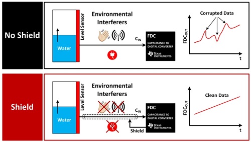
Have you been experiencing problems with fluctuations in capacitance measurements within your sensor system? There are several explanations for these fluctuations, but the most common root cause is external parasitic capacitance interference. This interference, for example unintentional hand proximity or EMI from the surrounding area, requires attention and should be addressed in system design, since it can significantly reduce system reliability and sensitivity. Fortunately, there are ways to help mitigate these factors so that they do not affect capacitance-measurement readings; one of those ways is through active shielding. The FDC1004 features active shield drivers that can reduce interference and help focus the sensing field of a capacitive sensor.

Imagine a wire connected to one of the channel inputs of the FDC1004. As your hand approaches the wire and comes into contact with it, your hand forms a closed loop with the signal on the wire, since the human body acts as a grounded source. If your hand is not the intended target, it is considered a parasitic capacitance. The solution: an active shield wrapped around the wire. The shield driver is an active signal output that is driven at the same voltage potential (same waveform) as the sensor input, so there is no potential difference – and thus no capacitance – between the shield and sensor input. Any external interference will couple the shield signal with minimal interaction with the sensor signal. Figure 1 shows how shielding the signal line from sensor to the FDC1004 will reduce any interferers from affecting capacitance measurements.

Figure 1: Shield versus no shield comparison

There are several benefits to using a shield in capacitive-sensing applications:

  • It directs and focuses the sensing zone to a particular area.
  • It reduces and eliminates parasitic capacitances and interferers.
  • It eliminates temperature variation effects on the ground plane.

Directivity with a shield

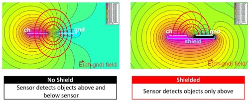
With no shield, the sensor, CH, detects objects above and below the sensor. Depending on the application, detection above and below may not be acceptable and can misrepresent the capacitance measurements relative to a target. By using a shield sensor underneath the CH and GND electrodes, the field lines below are essentially blocked; only the top field lines have a defined path. The example shown in Figure 2 is somewhat simplified and does not include fringing effects.

Figure 2: Electric field lines between CH and GND

Parasitic capacitance and interferers

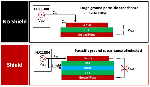
Good system-level design principles require a ground plane to help reduce noise and increase signal integrity. For capacitive-sensing applications, a ground plane becomes an issue because it creates a termination source for electric field lines, even though the ground plane is not where the intended sensing area should be. If the printed circuit board (PCB) stack up is similar to that shown in Figure 3, fringing effects will occur and cause the measurements to include the capacitance path from the sensor to the ground plane. This large ground parasitic capacitance can be reduced significantly with a shield plane between the sensor and ground plane.

In an ideal case, the shield will eliminate all influence from the ground plane; but because of fringing effects, a small parasitic ground capacitance amount will still exist in the measurements. The shield size would have to be much greater than the size of the sensor and ground plane so that the field lines on the edges are much weaker compared to the overall capacitance measurement.

Figure 3: Ground-plane effects with and without shielding

Temperature effects on ground planes

Temperature is a factor that causes the parasitic ground plane capacitance to vary in addition to the initial parasitic capacitance offset it introduces into the measurements. This is seen as an offset that is time-varying. These variations from temperature are caused by expansion and contraction of the ground plane. Inserting a shield plane between the sensor and ground plane helps mitigate the influence of the parasitic ground plane capacitance from the measurements.

Typical implementation with the FDC1004

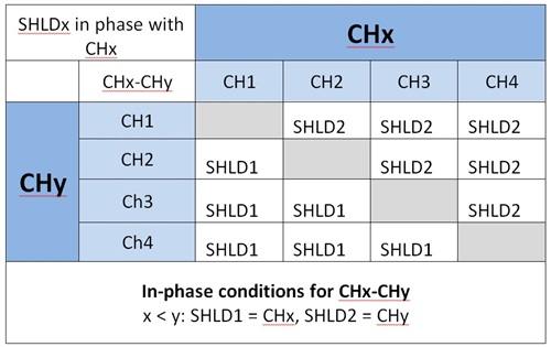
The FDC1004 has the capability to drive a 400pF load on the shield driver pins. Any load greater than 400pF will cause the shield to not function properly and effectively. Pairing the input channels with a shield depends on the mode of operation. In single-ended mode, CIN1 through CIN4 can be paired with either SHLD1 or SHLD2, because the two shield pins are shorted internally. For differential mode, Table 1 lists the in-phase conditions.

Table 1: Channel and shield pairing for differential mode

For example, if the FDC1004 is configured so that CH1-CH4, CH1 would be in-phase and paired with SHLD1, while CH4 would be in-phase and paired with SHLD2.

Stay tuned for part 2 of this series to learn more about shield sensor design, and how the size and placement of the shield in relation to the sensor electrode affects sensor performance.

Additional resources:


How to save power using load switches

$
0
0

Thanks to the Internet of Things revolution, we’re seeing more devices connected to the cloud via Wi-Fi®  and Bluetooth®. Load switches are commonly used to save power by disabling radios (and other power-hungry subsystems) when your smartphone, for example, is in standby mode. This lowers the device’s overall power consumption, making batteries last longer.

How does a load switch work?

Think of a load switch as an electronic light switch, used to turn a load on and off. Basic load switches have only four pins: VIN, VOUT, ON and GND. Figure 1 shows features found in more complex load switches.) Turning the load switch on (by asserting ON high) lets current flow from VIN to VOUT. When you turn off the switch, no current flows from VIN to VOUT, and everything downstream is also turned off. The standby power consumption of the load switch effectively replaces the standby power consumption of the load(s) on VOUT

Figure 1: Generic load switch block diagram

How much power do you really save?

For a real-world example, let’s assume we have a WiFi or Bluetooth radio which consumes approximately 5µA in sleep mode.   I will be using the TPS22915 load switch to compare the power savings with and without a load switch. Without the load switch, our power consumption when the radio is in its standby or sleep mode would be around 5µA, as mentioned earlier.  In the TPS22915’s data sheet, typical ISD (shutdown current) is 0.5µA (not to be confused with the IQ or quiescent current rating of 7.7µA, which is the load switch’s active power consumption). Adding the TPS22915 (Figure 2), consumes 10x less power!

Figure 2: Comparison of standby power consumption with and without a load switch

Now let’s assume that our Wi-Fi chip has a bit lower performance, and consumes closer to 250µA when in its standby or sleep mode. Adding the TPS22915 now consumes 500x less power! By saving power, you can shrink your end equipment by using smaller batteries, or have them last longer between recharges. 

Which load switch is right for you?

When selecting a load switch, it is important to ensure that it has the correct rating for your application. Pay close attention to the maximum voltage, maximum current and ON-resistance (RON). After confirming that the load switch is rated for the correct voltage and current, decide how much power loss (V=IR drop) is acceptable. TI offers a wide array of load switches to choose from; the latest in the family is the TPS22915. The TPS22915 has a typical RON of 38mΩ. For a 1.5A load, the voltage drop across the load switch is 57mV (V=1.5A * 38mΩ). Applying 3.3V, 1.5A to VIN, the VOUT will be ~3.24V.

As load current increases, the RON of the load switch becomes increasingly important because voltage drop scales with current. This is why it’s important that the TPS22915 has 31% lower RON at 3.3V than similar load switches. Without the TPS22915, VOUT would be ~3.21V instead of 3.24V. Figure 3 compares RON across VIN.

Figure 3: RON comparison across VIN for leading 5.5V WCSP-4 load switches

If you’re hungry to learn more about load switches, I encourage you to dive into the Basics of Load Switches app note and join the TI E2E™ Community load switches forum to search for solutions and hear from experts. 

What are you sensing? Active shielding for capacitive sensing, part 2

$
0
0

Thanks for tuning into part 2 of this series on active shielding. In my last post, I talked about the benefits of shielding and how it helps mitigate parasitic-capacitance interference from your capacitance measurements. Today, I’ll discuss shield sensor designs and how the size and placement of the shield in relation to the sensor electrode affects sensor performance.

The shape and position of the shield relative to the sensor is an important factor in capacitive-sensor design. The sensing angle without a shield, as shown in Figure 1, picks up any stray interference within the field-line vicinity. The sensing angle with a shield depends on both how large the shield is compared to the sensor and how close the shield is to the sensor. Although the shield helps mitigate the effects of parasitic-capacitance interference from the surrounding area, it does reduce the sensitivity and overall dynamic range of the system.

Figure 1: Direct/focusing the sensing area

I performed an experiment with four different shielding configurations to determine what kind of relationship shielding has with directivity, sensitivity and parasitic-capacitance interference mitigation. The isolated sensor topology employed here is mainly used for proximity and gesture-recognition applications such as system wakeup detection and infotainment display interaction. The target object is the human hand (grounded target). The four configurations were:

  1. CIN1 electrode only.
  2. Shield1 the same size as CIN1 and directly underneath.
  3. Shield1 200% larger than CIN1 and directly underneath.
  4. Shield1 ring added on the same plane as CIN1 with Shield1 underneath (same as configuration 3).

Figure 2: Sensor layouts

Figure 2 shows the top and side profiles of the sensor layout stack-up. Shielding the sensor electrode will help block any external interference and noise. The experimental results show that even though shielding does not totally eliminate all of the interference, it does significantly reduce it. The top side of the sensors is the intended target area for the human hand (in proximity and gesture-recognition applications). The top side is the most common direction for proximity detection, whereas the proximity from the side and the bottom is treated as the unwanted interference.

Figure 3: Interference data comparison from the side

Figure 3 shows the change in capacitance as the parasitic capacitance (human hand) approaches from the side of the sensors. It is apparent that as the shield size increases, the effects of the interference are reduced.

Figure 4: Sensitivity data comparison from the top

Figure 4 displays the sensitivity of the sensors from the intended target direction (from the top). Note that increasing the area of the shield decreases sensitivity and dynamic range to some extent in the target zone. This occurs because the shield decreases the amount of electric field lines that terminate to the nearest ground source. Various applications will require a certain proximity range and margin for interference; the shield will need to be sized appropriately for each case since it does not have a linear relationship to range and interference. Table 1 shows that either using a shield the same size as the sensor, or one that is 200% larger in area, has about the same impact on target-zone sensitivity. But using a larger shield can reduce the vulnerability to interference from the side.

Measurements with bottom-side interference show a significant reduction in capacitance change at a fixed distance away from the sensor. All of the interference cannot be eliminated unless the shield is much larger (by an order of magnitude) than the sensor due to fringing fields near the edges of the electrodes.

Table 1: Error-reduction comparison

Overall, shielding is a very effective method for protecting the signal integrity of the system. The placement and configuration of the shield depends on the application and amount of acceptable parasitic capacitance. Up to 77% of parasitic-capacitance interference can be eliminated at an expense of up to 74% decreased sensitivity, depending on the desired sensing range and shield configuration. You will need to characterize each system properly to determine the optimal shield parameters.

Additional resources:


JESD204B: How to measure and verify your deterministic latency

$
0
0

In my last post, I presented a three-step process for calculating the deterministic latency of a JESD204B link. In this post, I’ll explain: 1) how to choose your release buffer delay (RBD) to ensure a deterministic latency, and 2) how to measure and verify the expected deterministic latency. 

Choosing the appropriate RBD value

As discussed in my previous post, RBD=K is the default setting. This allows the initial lane alignment sequence to align all lanes and release them at the subsequent multiframe boundary. There are situations where system delays could cause the last arriving lane to straddle the data release point. In this case, the lanes may be released with a latency that varies by one multiframe period, depending on if the last lane arrives just before or just after the multiframe boundary. The choice of RBD is critical in this situation to provide enough margin to account for variations in the system delay while at the same time minimizing latency when the data is released.

Figure 1: Possible release points A: maximum margin, maximum delay versus B: minimum margin, minimum delay

As shown in Figure 1, an RBD=A setting would provide possible release points that would maximize the margin for variations in system delay. This also means, however, that the data must be delayed longer before it is released, resulting in a longer latency. A setting of RBD=B would release the data immediately after the last lane arrival, but some care is required to ensure that the selected delay allows enough margin to avoid possible issues with system variations.

Figure 2: Adjusting RBD to find a possible optimal release point 

One possible setting would be to offset the release point by the expected amount of system variation after the latest arriving lane. This may provide the appropriate trade-off between latency and margin to absorb possible system variations. This optimal data release point can be derived from the system parameters if those are readily available. For cases where the delay parameters are not readily available, you can derive the release point empirically.

First, start by using the default RBD=K setting. Then repeat the power cycle and adjust the delay until you observe full multiframe jumps in the measured latency. This is the upper range of the last lane arrival. As you continue to decrease the RBD value through the delays caused by system variation, you will notice the latency stabilize. This is the lower range of the last lane arrival. The difference between the upper and lower range is the system delay variation. Setting the RBD delay to this offset from the upper range is one possible optimal solution that would provide a margin against system variations while providing a consistent data release point.

Calculating, measuring and verifying your deterministic latency

A system consisting of the 16-bit, 370-MSPS ADC16DX370 and an FPGA was used to compare the measured latency with the expected latency from our calculations. The ADC16DX370 was connected to the FPGA mezzanine card (FMC) port of the FPGA platform. A pulse was generated and fed into the input of the analog-to-digital converter (ADC), as well as an oscilloscope. The ADC samples the input signal and passes this data to the FPGA through the JESD204B link. Upon receiving the ADC sample, the FPGA then sends the most significant bit (MSB) to an input/output (I/O) pin to be monitored by the oscilloscope. By factoring in the delays of the cables and board traces, and the time it takes for the input pulse signal to be sampled and passed through the link to the FPGA, it is possible to measure and confirm your latency.

The block diagram in Figure 3 shows the expected delays of the cables and traces for the various parts of the setup.

Figure 3: Additional non-device-related delays used in the delay calculation. A pulse is sent to the oscilloscope and the ADC. The MSB from the captured sample is compared against the pulse to measure the delay.

The following configuration was used on the ADC16DX370 and FPGA:

  1. ADC device clock = 370MSPS (2.7ns period).
  2. JESD204B parameters:
    1. L = 4, M = 2, F = 1, S = 1, K = 32.
    2. The frame cycle = 10*F/linerate = 10*1/3700MSPS = 2.7ns.
    3. LMFC cycle = frame cycle * K = 2.7ns*32 = 86.4ns.
  3. FPGA device clock = 92.5MHz (10.8ns).
  4. Link parameters (frame cycles):
    1. .
    2. N = 2, RBD = 28 (less than K).
  5. Additional delays outside of the link latency (frame cycles):
    1. ADC core delay = 12.5.
    2. DEVCLK routing skew and MSB output cable/printed circuit board (PCB) routing delay = 3.8ns/2.7ns ~ 1.4.
    3. SYSREF/DEVCLK sampling skew within ADC = 1.5.
    4. FPGA receiver processing delays to latch the samples and send out the MSB = ~7.

As derived in my previous post, Equation 1 is:

Link latency = 116.5 frame cycles

Estimated total latency = link latency + additional delays = 116.5 + 12.5 + 1.4 + 1.5 + 7 = 138.9 cycles

The delay was measured over multiple power cycles between the signal pulse and the MSB from the FPGA. This gave a consistent latency result of 379.6ns, which equates to 140.4 frame cycles. This closely matches the estimated delay of 139 cycles based on the system parameters.

For additional advice about designing with for JESD204B, see the resources below:


Differential to single ended: What happens when you use only one differential amplifier output

$
0
0

Many applications require the conversion of a differential signal to single ended. Some common examples are an RF DAC buffer or a coaxial cable driver.  Most of the time you can accomplish this with a magnetic transformer, but sometimes a transformer won’t work. If that’s the case, can you use a fully differential amplifier (FDA)? The answer is a definite maybe.

As a refresher, an FDA has two distinct outputs available. The first output is the most commonly used: it consists of the difference between the outputs, . The other output is generally considered a parasitic output; it is the average value of the two outputs . The common-mode output DC level is important; however, its derivative should be zero, meaning that it should have no AC component. This, in fact, will not be the case.

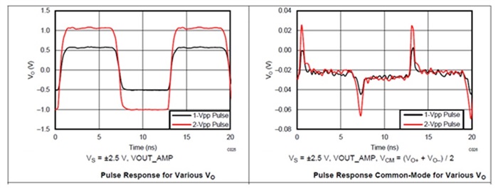
Let’s look at an example scenario. The LMH5401 is an FDA with extraordinarily high bandwidth. The pulse response is shown in Figure 1. At left is the differential output response, and at right is the common-mode response.

Figure 1: LMH5401 pulse response, differential (left) and common mode (right)

Now that we have reviewed the two main output modes of an FDA, let’s look at two potential alternative outputs: Out+ alone and Out- alone. For now, let’s use the identity of  and look at what happens to the two primary responses with respect to one output only. For an FDA, the closed-loop gain = ) ; given the same loop gain using only one output, the closed-loop gain  .This makes it clear that using only one amplifier output cuts the gain by 6dB, or by a factor of two. With an amplifier like the LMH5401, you can mitigate this drawback by using different external resistors to set the amplifier gain higher by a factor of two.  Similarly, if you are using FDAs as attenuators, this gain reduction is an added benefit.  

Using the same method, the amplifier common mode would change from to  . This conversion shows that when using the single-ended method, the amplifier output common mode is no longer a meaningful concept since the common mode is simply equal to the output

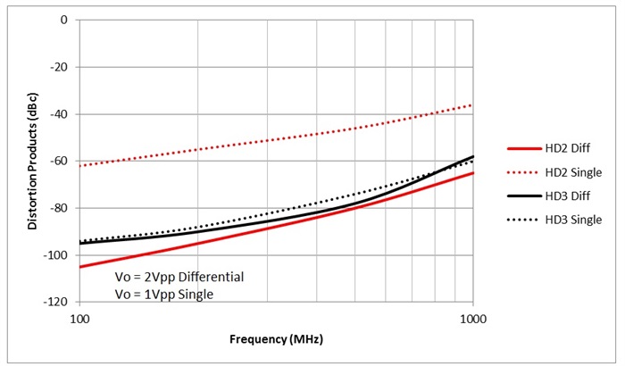
To gain more insight into the amplifier performance, we’ll need to use more sensitive equipment than that used for Figure 1. With a spectrum analyzer, we can measure the amplifier distortion under single-tone conditions with a very high degree of precision. Figure 2 shows distortion measurements for the LMH5401.

Figure 2: Distortion measured with differential and single-ended outputs

Figure 2 clearly shows that the single-ended output does not provide the linearity of a differential condition. The output voltage for both conditions is 2Vpp. Note that in the single-ended output condition, one output running 2Vpp is the “same” as a 4Vpp condition for a differential output.

Given this serious handicap of single-ended operation, what happens when we drop the signal amplitude to make the conditions more comparable? Figure 3 shows what happens when you decrease the signal amplitude so that each output is swinging the same voltage, whether the results are measured in single ended or differential mode.

Figure 3: Distortion measured with differential and single-ended outputs

Figure 3 clearly shows that the third-order distortion products (HD3) are very similar for a single-ended output or a differential output – as long as you account for the amplitude penalty of single-ended outputs. The results for the second-order distortion products (HD2) are not comparable, however. This is the primary disadvantage of using an FDA with only a single output. While the HD2 of each output will cancel when the outputs are combined into a differential signal, this does not happen with a single-ended output.

Figure 4: Test schematic

In conclusion, using a single output from an FDA may work in some limited applications: when the signal is at the lower end of the amplifier’s working frequency range, when the signal amplitudes are small, and when second-order distortion products are not a primary performance metric.

Related technical resources:


A race against the clock: how to determine the power-up states of clocked devices

$
0
0

Many engineers choose flip-flops, shift registers, or other clocked devices for temporary storage and moving small amounts of data. These clocked devices have one or more clock-input pins, typically designated CLK or CP. A clock edge will determine when a specific function occurs; for example, the data may be clocked to an output, or data may be moved from one pin to another. Device data sheets specify whether this happens on the positive or negative edge, and include a truth table for each part.

Often, these truth tables include up and down arrows indicating the clock status. But what happens in that mysterious state before any clock edge has occurred? Consider the SN74AUP1G80, a five-pin D-type flip-flop. If VCC powers up and there is no valid clock edge, the truth table says that the Ǭ output is equal to Ǭ0.

Not very helpful, is it? Actually, it illustrates a design reality. We don’t know what the output will be before the first valid clock edge. When the device turns on, thresholds on internal transistors in the clocked device can float to indeterminate values, resulting in unpredictable signal levels at Ǭ. Typically, under the same conditions, the part will start up with the same output value, but this can vary across temperature and manufacturing lot to another. Therefore, for these clocked devices, it is imperative to wait until VCC has ramped to an appropriate level and a valid clock edge has passed before reading the output.

If the clock edge on a positive-edge-triggered device rises with VCC, I recommend waiting an extra clock cycle, as the clock threshold changes with VCC and any small amount of noise can cause unwanted clocking.

One clever trick you can use to “beat the clock” is to use devices with clear (CLR) (set all outputs to 0) and preset (PRE) (set all outputs to 1) inputs. Typically, in TI data sheets we designate these pins by some form of PRE, CLR or MR (for master reset). Look at the SN74AUP1G74, for example. The active-low CLR and PRE inputs allow engineers to override the clock! When used, these pins allow you to set the output of the device before CLK, giving you more control over the output bus. 

For more advice on powering clocked devices, review these additional resources:

Viewing all 408 articles
Browse latest View live


<script src="https://jsc.adskeeper.com/r/s/rssing.com.1596347.js" async> </script>